- 您現在的位置:買賣IC網 > PDF目錄373914 > AD7707EB (Analog Devices, Inc.) 3 V/5 V 610 V Input Range 1 mW 3-Channel 16-Bit Sigma-Delta ADC(316.51 k) PDF資料下載
參數資料
| 型號: | AD7707EB |
| 廠商: | Analog Devices, Inc. |
| 英文描述: | 3 V/5 V 610 V Input Range 1 mW 3-Channel 16-Bit Sigma-Delta ADC(316.51 k) |
| 中文描述: | 3伏/ 5伏610 V輸入范圍1毫瓦3通道16位Σ-Δ模數轉換器(316.51十一) |
| 文件頁數: | 20/40頁 |
| 文件大小: | 316K |
| 代理商: | AD7707EB |
第1頁第2頁第3頁第4頁第5頁第6頁第7頁第8頁第9頁第10頁第11頁第12頁第13頁第14頁第15頁第16頁第17頁第18頁第19頁當前第20頁第21頁第22頁第23頁第24頁第25頁第26頁第27頁第28頁第29頁第30頁第31頁第32頁第33頁第34頁第35頁第36頁第37頁第38頁第39頁第40頁
REV. A
AD7707
–20–
ANALOG INPUT
Analog Input Ranges
The AD7707 contains two low level pseudo-differential analog
input channels AIN1 and AIN2. These input pairs provide
programmable-gain, differential input channels that can handle
either unipolar or pseudo bipolar input signals. It should be
noted that the bipolar input signals are referenced to the
LOCOM input. The AD7707 also has a high level analog input
channel AIN 3 which is referenced to HICOM. Figure 11
shows the input structure on the high level input channel.
In normal 5 V operation VBIAS is normally connected to 2.5 V
and HICOM is connected to AGND. This arrangement ensures
that the voltages seen internally are within the common-mode
range of the buffer in buffered mode and within the supply
range in unbuffered mode. This device can be programmed to
operate in either buffered or unbuffered mode via the BUF bit
in the setup register. Note that the signals on AIN3 are with
respect to the HICOM input and not with respect to AGND or
DGND.
The differential voltage seen by the AD7707 when using the
high level input channel is the difference between AIN3(+) and
AIN3(–) on the mux as shown in Figure 11.
AIN
3(+) = (
AIN
3 + 6
×
VBIAS
+
V
(
HICOM
))/8
AIN3
MUX
VBIAS
1R = 5k
V
6R
6R
3R
1R
HICOM
AIN3(–)
AIN3(+)
Figure 11. AIN3 Input Structure
AIN
3(–) =
V
(
HICOM
) + 0.75
×
(
VBIAS
–
V
(
HICOM
))
In unbuffered mode, the common-mode range of the low level
input channels is from AGND – 100 mV to AV
DD
+30 mV.
This means that in unbuffered mode the part can handle both
unipolar and bipolar input ranges for all gains. Absolute volt-
ages of AGND – 100 mV can be accommodated on the analog
inputs without degradation in performance, but leakage current
increases appreciably with increasing temperature. In buffered
mode, the analog inputs can handle much larger source imped-
ances, but the absolute input voltage range is restricted to be-
tween AGND+ 50 mV to AV
DD
– 1.5 V which also places
restrictions on the common-mode range. This means that in
buffered mode there are some restrictions on the allowable
gains for bipolar input ranges. Care must be taken in setting up
the common-mode voltage and input voltage range so that the
above limits are not exceeded, otherwise there will be a degra-
dation in linearity performance.
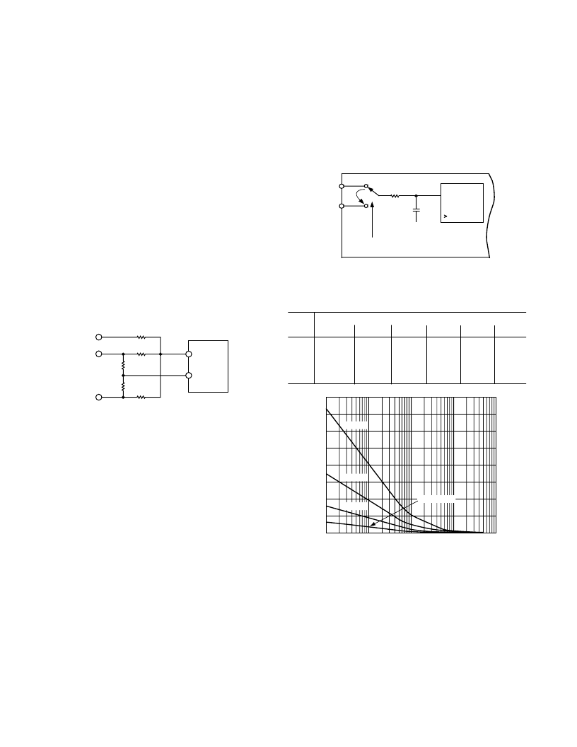
In unbuffered mode, the analog inputs look directly into the
7pF input sampling capacitor, C
SAMP
. The dc input leakage
current in this unbuffered mode is 1nA maximum. As a result,
the analog inputs see a dynamic load that is switched at the
input sample rate (see Figure 12). This sample rate depends on
master clock frequency and selected gain. C
SAMP
is charged to
AIN(+) and discharged to AIN(–) every input sample cycle.
The effective on-resistance of the switch, R
SW
, is typically 7 k
.
C
SAMP
must be charged through R
SW
and any additional source
impedances every input sample cycle. Therefore, in unbuffered
mode, source impedances mean a longer charge time for C
SAMP
and this may result in gain errors on the part. Table XVI shows
the allowable external resistance/capacitance values, for unbuffered
mode, such that no gain error to the 16-bit level is introduced
on the part. Note that these capacitances are total capacitances
on the analog input. This external capacitance includes 10 pF
from pins and lead frame of the device.
AIN(+)
AIN(–)
SWITCHING FREQUENCY DEPENDS ON
f
CLKIN
AND SELECTED GAIN
R
SW
(7k
V
TYP)
C
(7pF)
FIRST
INTEGRATOR
HIGH INPUT
IMPEDANCE
1G
V
DD
/2
Figure 12. Unbuffered Analog Input Structure
Table XVI. External R, C Combination for No 16-Bit Gain
Error on Low Level Input Channels (Unbuffered Mode Only)
External Capacitance (pF)
50
100
Gain
0
500
1000
5000
1
2
4
8–128
368 k
177.2 k
44.2 k
82.8 k
35.2 k
90.6 k
54.2 k
14.6 k
8.2 k
26.4 k
7.2 k
12.6 k
3.4 k
5.8 k
1.58
2.2 k
1.12 k
4 k
1.94 k
540
880
21.2 k
9.6 k
240
EXTERNAL CAPACITANCE – pF
0
10000
E
V
10
100
1000
0
50
100
150
200
250
300
350
400
GAIN = 1
GAIN = 4
GAIN = 8-128
GAIN = 2
Figure 13. External R, C Combination for No 16-Bit Gain
Error on Low Level Input Channels (Unbuffered Mode Only)
In buffered mode, the analog inputs look into the high imped-
ance inputs stage of the on-chip buffer amplifier. C
SAMP
is
charged via this buffer amplifier such that source impedances do
not affect the charging of C
SAMP
. This buffer amplifier has an
offset leakage current of 1 nA. In buffered mode, large source
impedances result in a small dc offset voltage developed across
the source impedance, but not in a gain error.
相關PDF資料 |
PDF描述 |
|---|---|
| AD7708BR | Shaft; Style: 2 - light; Applicable Model: LE-P / LEL-W |
| AD7708BRU | 8-/10-Channel, Low Voltage, Low Power, ADCs |
| AD7708 | 8-/10-Channel, Low Voltage, Low Power, ADCs |
| AD7718 | 8-/10-Channel, Low Voltage, Low Power, ADCs |
| AD7718BR | 8-/10-Channel, Low Voltage, Low Power, ADCs |
相關代理商/技術參數 |
參數描述 |
|---|---|
| AD7708 | 制造商:AD 制造商全稱:Analog Devices 功能描述:8-/10-Channel, Low Voltage, Low Power, ADCs |
| AD7708BR | 功能描述:IC ADC 16BIT R-R 8/10CH 28-SOIC RoHS:否 類別:集成電路 (IC) >> 數據采集 - 模數轉換器 系列:- 標準包裝:1,000 系列:- 位數:16 采樣率(每秒):45k 數據接口:串行 轉換器數目:2 功率耗散(最大):315mW 電壓電源:模擬和數字 工作溫度:0°C ~ 70°C 安裝類型:表面貼裝 封裝/外殼:28-SOIC(0.295",7.50mm 寬) 供應商設備封裝:28-SOIC W 包裝:帶卷 (TR) 輸入數目和類型:2 個單端,單極 |
| AD7708BR-REEL | 功能描述:IC ADC 16BIT R-R 8/10CH 28-SOIC RoHS:否 類別:集成電路 (IC) >> 數據采集 - 模數轉換器 系列:- 標準包裝:1,000 系列:- 位數:16 采樣率(每秒):45k 數據接口:串行 轉換器數目:2 功率耗散(最大):315mW 電壓電源:模擬和數字 工作溫度:0°C ~ 70°C 安裝類型:表面貼裝 封裝/外殼:28-SOIC(0.295",7.50mm 寬) 供應商設備封裝:28-SOIC W 包裝:帶卷 (TR) 輸入數目和類型:2 個單端,單極 |
| AD7708BR-REEL7 | 功能描述:IC ADC 16BIT R-R 8/10CH 28-SOIC RoHS:否 類別:集成電路 (IC) >> 數據采集 - 模數轉換器 系列:- 標準包裝:1,000 系列:- 位數:16 采樣率(每秒):45k 數據接口:串行 轉換器數目:2 功率耗散(最大):315mW 電壓電源:模擬和數字 工作溫度:0°C ~ 70°C 安裝類型:表面貼裝 封裝/外殼:28-SOIC(0.295",7.50mm 寬) 供應商設備封裝:28-SOIC W 包裝:帶卷 (TR) 輸入數目和類型:2 個單端,單極 |
| AD7708BRU | 功能描述:IC ADC 16BIT R-R 8/10CH 28-TSSOP RoHS:否 類別:集成電路 (IC) >> 數據采集 - 模數轉換器 系列:- 標準包裝:1,000 系列:- 位數:16 采樣率(每秒):45k 數據接口:串行 轉換器數目:2 功率耗散(最大):315mW 電壓電源:模擬和數字 工作溫度:0°C ~ 70°C 安裝類型:表面貼裝 封裝/外殼:28-SOIC(0.295",7.50mm 寬) 供應商設備封裝:28-SOIC W 包裝:帶卷 (TR) 輸入數目和類型:2 個單端,單極 |
發布緊急采購,3分鐘左右您將得到回復。