- 您現在的位置:買賣IC網 > PDF目錄373914 > AD7712* (Analog Devices, Inc.) Rail-to-Rail, Very Low Noise Universal Dual Filter Building Block; Package: SSOP; No of Pins: 16; Temperature Range: 0°C to +70°C PDF資料下載
參數資料
| 型號: | AD7712* |
| 廠商: | Analog Devices, Inc. |
| 英文描述: | Rail-to-Rail, Very Low Noise Universal Dual Filter Building Block; Package: SSOP; No of Pins: 16; Temperature Range: 0°C to +70°C |
| 中文描述: | LC2MOS信號調理模數轉換器 |
| 文件頁數: | 12/28頁 |
| 文件大小: | 229K |
第1頁第2頁第3頁第4頁第5頁第6頁第7頁第8頁第9頁第10頁第11頁當前第12頁第13頁第14頁第15頁第16頁第17頁第18頁第19頁第20頁第21頁第22頁第23頁第24頁第25頁第26頁第27頁第28頁
REV. E
–12–
AD7712
CIRCUIT DESCRIPTION
The AD7712 is a sigma-delta A/D converter with on-chip digital
filtering, intended for the measurement of wide dynamic range,
low frequency signals such as those in industrial control or pro-
cess control applications. It contains a sigma-delta (or charge
balancing) ADC, a calibration microcontroller with on-chip
static RAM, a clock oscillator, a digital filter and a bidirectional
serial communications port.
The part contains two analog input channels, one programmable
gain differential input and one programmable gain high level
single-ended input. The gain range on both inputs is from 1 to
128. For the AIN1 input, this means that the input can accept
unipolar signals of between 0 mV to +20 mV and 0 mV to
+2.5 V or bipolar signals in the range from
±
20 mV to
±
2.5 V
when the reference input voltage equals +2.5 V. The input volt-
age range for the AIN2 input is
±
4
×
V
REF
/GAIN and is
±
10 V with
the nominal reference of +2.5 V and a gain of 1. The input
signal to the selected analog input channel is continuously
sampled at a rate determined by the frequency of the master
clock, MCLK IN, and the selected gain (see Table III). A
charge balancing A/D converter (Sigma-Delta Modulator) con-
verts the sampled signal into a digital pulse train whose duty
cycle contains the digital information. The programmable gain
function on the analog input is also incorporated in this sigma-
delta modulator with the input sampling frequency being modi-
fied to give the higher gains. A sinc
3
digital low-pass filter
processes the output of the sigma-delta modulator and updates
the output register at a rate determined by the first notch fre-
quency of this filter. The output data can be read from the serial
port randomly or periodically at any rate up to the output regis-
ter update rate. The first notch of this digital filter (and hence its
–3 dB frequency) can be programmed via an on-chip control
register. The programmable range for this first notch frequency
is from 9.76 Hz to 1.028 kHz, giving a programmable range for
the –3 dB frequency of 2.58 Hz to 269 Hz.
The basic connection diagram for the part is shown in Figure 3.
This shows the AD7712 in the external clocking mode with both
the AV
DD
and DV
DD
pins of the AD7712 being driven from the
analog +5 V supply. Some applications will have separate sup-
plies for both AV
DD
and DV
DD
, and in some of these cases, the
analog supply will exceed the +5 V digital supply (see Power
Supplies and Grounding section).
REF IN(+)
V
BIAS
REF OUT
AIN1(+)
AIN1(–)
AIN2
AGND
V
SS
DGND
MCLK IN
MCLK OUT
MODE
SCLK
SDATA
REF IN(–)
A0
DIFFERENTIAL
ANALOG INPUT
SINGLE-ENDED
ANALOG INPUT
ANALOG
GROUND
DIGITAL
GROUND
DATA
READY
TRANSMIT
(WRITE)
RECEIVE
(READ)
SERIAL
DATA
SERIAL
CLOCK
ADDRESS
INPUT
+5V
AD7712
10
m
F
0.1
m
F
ANALOG
+5V SUPPLY
AV
DD
DV
DD
DV
DD
STANDBY
SYNC
DRDY
TFS
RFS
0.1
m
F
Figure 3. Basic Connection Diagram
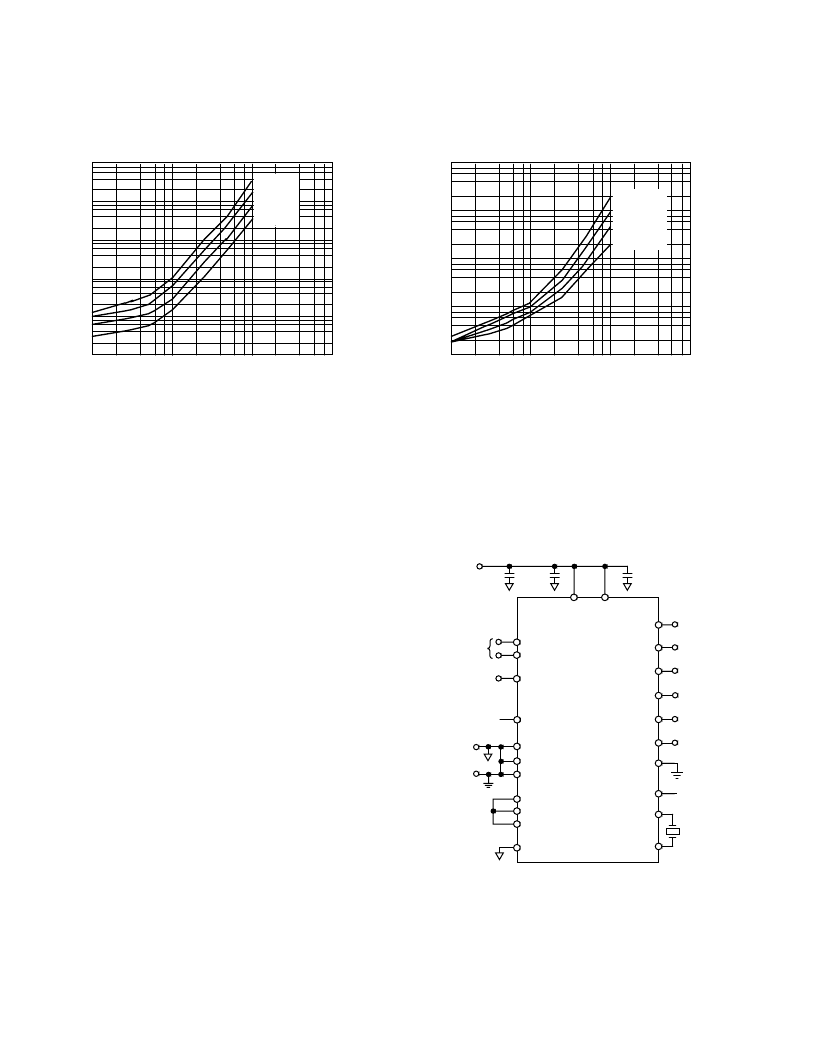
1000
10
0.1
10
1000
10000
100
1
100
NOTCH FREQUENCY – Hz
O
m
V
GAIN OF 16
GAIN OF 32
GAIN OF 64
GAIN OF 128
Figure 2b. Plot of Output Noise vs. Gain and Notch
Frequency (Gains of 16 to 128)
10000
100
0.1
10
1000
10000
GAIN OF 1
GAIN OF 2
GAIN OF 4
GAIN OF 8
1000
10
1
100
NOTCH FREQUENCY – Hz
O
m
V
Figure 2a. Plot of Output Noise vs. Gain and Notch
Frequency (Gains of 1 to 8)
Figures 2a and 2b give information similar to that outlined in Table I. In these plots, the output rms noise is shown for the full range
of available cutoffs frequencies rather than for some typical cutoff frequencies as in Tables I and II. The numbers given in these plots
are typical values at +25
°
C.
相關PDF資料 |
PDF描述 |
|---|---|
| AD7712 | Signal Conditioning ADC(LC2MOS信號調節A/D轉換器) |
| AD7713* | LC2MOS Loop-Powered Signal Conditioning ADC |
| AD7713AN | LC2MOS Loop-Powered Signal Conditioning ADC |
| AD7713AQ | LC2MOS Loop-Powered Signal Conditioning ADC |
| AD7713AR | LC2MOS Loop-Powered Signal Conditioning ADC |
相關代理商/技術參數 |
參數描述 |
|---|---|
| AD7712_04 | 制造商:AD 制造商全稱:Analog Devices 功能描述:LC2MOS Signal Conditioning ADC |
| AD7712AN | 功能描述:IC ADC SIGNAL COND LC2MOS 24-DIP RoHS:否 類別:集成電路 (IC) >> 數據采集 - 模數轉換器 系列:- 標準包裝:1 系列:- 位數:14 采樣率(每秒):83k 數據接口:串行,并聯 轉換器數目:1 功率耗散(最大):95mW 電壓電源:雙 ± 工作溫度:0°C ~ 70°C 安裝類型:通孔 封裝/外殼:28-DIP(0.600",15.24mm) 供應商設備封裝:28-PDIP 包裝:管件 輸入數目和類型:1 個單端,雙極 |
| AD7712ANZ | 功能描述:IC ADC SIGNAL COND LC2MOS 24-DIP RoHS:是 類別:集成電路 (IC) >> 數據采集 - 模數轉換器 系列:- 其它有關文件:TSA1204 View All Specifications 標準包裝:1 系列:- 位數:12 采樣率(每秒):20M 數據接口:并聯 轉換器數目:2 功率耗散(最大):155mW 電壓電源:模擬和數字 工作溫度:-40°C ~ 85°C 安裝類型:表面貼裝 封裝/外殼:48-TQFP 供應商設備封裝:48-TQFP(7x7) 包裝:Digi-Reel® 輸入數目和類型:4 個單端,單極;2 個差分,單極 產品目錄頁面:1156 (CN2011-ZH PDF) 其它名稱:497-5435-6 |
| AD7712ANZ | 制造商:Analog Devices 功能描述:IC ADC 24-BIT SIGMA DELTA |
發布緊急采購,3分鐘左右您將得到回復。