- 您現在的位置:買賣IC網 > PDF目錄373914 > AD7712* (Analog Devices, Inc.) Rail-to-Rail, Very Low Noise Universal Dual Filter Building Block; Package: SSOP; No of Pins: 16; Temperature Range: 0°C to +70°C PDF資料下載
參數資料
| 型號: | AD7712* |
| 廠商: | Analog Devices, Inc. |
| 英文描述: | Rail-to-Rail, Very Low Noise Universal Dual Filter Building Block; Package: SSOP; No of Pins: 16; Temperature Range: 0°C to +70°C |
| 中文描述: | LC2MOS信號調理模數轉換器 |
| 文件頁數: | 19/28頁 |
| 文件大小: | 229K |
第1頁第2頁第3頁第4頁第5頁第6頁第7頁第8頁第9頁第10頁第11頁第12頁第13頁第14頁第15頁第16頁第17頁第18頁當前第19頁第20頁第21頁第22頁第23頁第24頁第25頁第26頁第27頁第28頁
2
–19–
REV. E
AD7712
Table VI. Calibration Truth Table
Cal Type
MD2, MD1, MD0
Zero-Scale Cal
Full-Scale Cal
Sequence
Duration
9
×
1/Output Rate
4
×
1/Output Rate
4
×
1/Output Rate
9
×
1/Output Rate
6
×
1/Output Rate
Self-Cal
System Cal
System Cal
System Offset Cal
Background Cal
0, 0, 1
0, 1, 0
0, 1, 1
1, 0, 0
1, 0, 1
Shorted Inputs
AIN
–
AIN
Shorted Inputs
V
REF
–
AIN
V
REF
V
REF
One Step
Two Step
Two Step
One Step
One Step
Measurement errors due to offset drift or gain drift can be elimi-
nated at any time by recalibrating the converter or by operating
the part in the background calibration mode. Using the system
calibration mode can also minimize offset and gain errors in the
signal conditioning circuitry. Integral and differential linearity
errors are not significantly affected by temperature changes.
POWER SUPPLIES AND GROUNDING
Since the analog inputs and reference input are differential,
most of the voltages in the analog modulator are common-mode
voltages. V
BIAS
provides the return path for most of the analog
currents flowing in the analog modulator. As a result, the V
BIAS
input should be driven from a low impedance to minimize errors
due to charging/discharging impedances on this line. When the
internal reference is used as the reference source for the part,
AGND is the ground return for this reference voltage.
The analog and digital supplies to the AD7712 are independent
and separately pinned out to minimize coupling between the
analog and digital sections of the device. The digital filter will
provide rejection of broadband noise on the power supplies,
except at integer multiples of the modulator sampling frequency.
The digital supply (DV
DD
) must not exceed the analog positive
supply (AV
DD
) by more than 0.3 V in normal operation. If sepa-
rate analog and digital supplies are used, the recommended
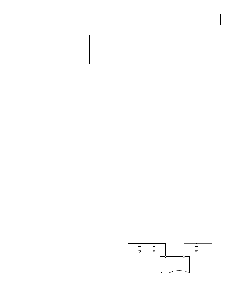
decoupling scheme is shown in Figure 10. In systems where
AV
DD
= +5 V and DV
DD
= +5 V, it is recommended that AV
DD
and DV
DD
are driven from the same +5 V supply, although each
supply should be decoupled separately as shown in Figure 10. It
is preferable that the common supply is the system’s analog +5 V
supply.
It is also important that power is applied to the AD7712 before
signals at REF IN, AIN or the logic input pins in order to avoid
excessive current. If separate supplies are used for the AD7712
and the system digital circuitry, then the AD7712 should be
powered up first. If it is not possible to guarantee this, then
current limiting resistors should be placed in series with the
logic inputs.
AD7712
0.1
m
F
0.1
m
F
10
m
F
ANALOG
SUPPLY
DIGITAL +5V
SUPPLY
AV
DD
DV
DD
Figure 10. Recommended Decoupling Scheme
Span and Offset Limits
Whenever a system calibration mode is used, there are limits on
the amount of offset and span that can be accommodated. The
range of input span in both the unipolar and bipolar modes for
AIN1 has a minimum value of 0.8
×
V
REF
/GAIN and a maxi-
mum value of 2.1
×
V
REF
/GAIN. For AIN2, both numbers are a
factor of four higher.
The amount of offset which can be accommodated depends on
whether the unipolar or bipolar mode is being used. This offset
range is limited by the requirement that the positive full-scale
calibration limit is
≤
1.05
×
V
REF
/GAIN for AIN1. Therefore,
the offset range plus the span range cannot exceed 1.05
×
V
REF
/
GAIN for AIN1. If the span is at its minimum (0.8
×
V
REF
/
GAIN) the maximum the offset can be is (0.25
×
V
REF
/GAIN)
for AIN1. For AIN2, both ranges are multiplied by a factor of
four.
In the bipolar mode, the system offset calibration range is again
restricted by the span range. The span range of the converter in
bipolar mode is equidistant around the voltage used for the zero-
scale point, thus the offset range plus half the span range cannot
exceed (1.05
×
V
REF
/GAIN) for AIN1. If the span is set to
2 ×
V
REF
/GAIN, the offset span cannot move more than
±
(0.05
×
V
REF
/GAIN) before the endpoints of the transfer function ex-
ceed the input overrange limits
±
(1.05
×
V
REF
/GAIN) for AIN1.
If the span range is set to the minimum
±
(0.4
×
V
REF
/GAIN),
the maximum
allowable offset range is
±
(0.65
×
V
REF
/GAIN)
for AIN1. Once again, for AIN2, both ranges are multiplied
by a factor of four.
POWER-UP AND CALIBRATION
On power-up, the AD7712 performs an internal reset which sets
the contents of the control register to a known state. However,
to ensure correct calibration for the device a calibration routine
should be performed after power-up.
The power dissipation and temperature drift of the AD7712 are
low and no warm-up time is required before the initial calibra-
tion is performed. However, if an external reference is being
used, this reference must have stabilized before calibration is
initiated.
Drift Considerations
The AD7712 uses chopper stabilization techniques to minimize
input offset drift. Charge injection in the analog switches and dc
leakage currents at the sampling node are the primary sources of
offset voltage drift in the converter. The dc input leakage cur-
rent is essentially independent of the selected gain. Gain drift
within the converter depends primarily upon the temperature
tracking of the internal capacitors. It is not affected by leakage
currents.
相關PDF資料 |
PDF描述 |
|---|---|
| AD7712 | Signal Conditioning ADC(LC2MOS信號調節A/D轉換器) |
| AD7713* | LC2MOS Loop-Powered Signal Conditioning ADC |
| AD7713AN | LC2MOS Loop-Powered Signal Conditioning ADC |
| AD7713AQ | LC2MOS Loop-Powered Signal Conditioning ADC |
| AD7713AR | LC2MOS Loop-Powered Signal Conditioning ADC |
相關代理商/技術參數 |
參數描述 |
|---|---|
| AD7712_04 | 制造商:AD 制造商全稱:Analog Devices 功能描述:LC2MOS Signal Conditioning ADC |
| AD7712AN | 功能描述:IC ADC SIGNAL COND LC2MOS 24-DIP RoHS:否 類別:集成電路 (IC) >> 數據采集 - 模數轉換器 系列:- 標準包裝:1 系列:- 位數:14 采樣率(每秒):83k 數據接口:串行,并聯 轉換器數目:1 功率耗散(最大):95mW 電壓電源:雙 ± 工作溫度:0°C ~ 70°C 安裝類型:通孔 封裝/外殼:28-DIP(0.600",15.24mm) 供應商設備封裝:28-PDIP 包裝:管件 輸入數目和類型:1 個單端,雙極 |
| AD7712ANZ | 功能描述:IC ADC SIGNAL COND LC2MOS 24-DIP RoHS:是 類別:集成電路 (IC) >> 數據采集 - 模數轉換器 系列:- 其它有關文件:TSA1204 View All Specifications 標準包裝:1 系列:- 位數:12 采樣率(每秒):20M 數據接口:并聯 轉換器數目:2 功率耗散(最大):155mW 電壓電源:模擬和數字 工作溫度:-40°C ~ 85°C 安裝類型:表面貼裝 封裝/外殼:48-TQFP 供應商設備封裝:48-TQFP(7x7) 包裝:Digi-Reel® 輸入數目和類型:4 個單端,單極;2 個差分,單極 產品目錄頁面:1156 (CN2011-ZH PDF) 其它名稱:497-5435-6 |
| AD7712ANZ | 制造商:Analog Devices 功能描述:IC ADC 24-BIT SIGMA DELTA |
發布緊急采購,3分鐘左右您將得到回復。