- 您現在的位置:買賣IC網 > PDF目錄373914 > AD7714* (Analog Devices, Inc.) 3 V/5 V. CMOS. 500 uA Signal Conditioning ADC PDF資料下載
參數資料
| 型號: | AD7714* |
| 廠商: | Analog Devices, Inc. |
| 英文描述: | 3 V/5 V. CMOS. 500 uA Signal Conditioning ADC |
| 中文描述: | 3 V / 5號五的CMOS。 500微安ADC的信號調理 |
| 文件頁數: | 29/40頁 |
| 文件大小: | 306K |
第1頁第2頁第3頁第4頁第5頁第6頁第7頁第8頁第9頁第10頁第11頁第12頁第13頁第14頁第15頁第16頁第17頁第18頁第19頁第20頁第21頁第22頁第23頁第24頁第25頁第26頁第27頁第28頁當前第29頁第30頁第31頁第32頁第33頁第34頁第35頁第36頁第37頁第38頁第39頁第40頁
2
AD7714
REV. C
–29–
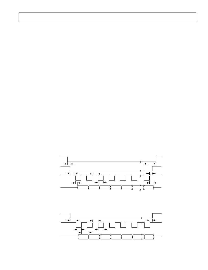
DIGITAL INTERFACE
The AD7714’s programmable functions are controlled using a
set of on-chip registers as previously outlined. Data is written to
these registers via the part’s serial interface, and read access to
the on-chip registers is also provided by this interface. All com-
munications to the part must start with a write operation to the
Communications Register. After power-on or
RESET
, the de-
vice expects a write to its Communications Register. The data
written to this register determines whether the next operation to
the part is a read or a write operation and also determines to
which register this read or write operation occurs. Therefore,
write access to any of the other registers on the part starts with a
write operation to the Communications Register followed by a
write to the selected register. A read operation from any register
on the part (including the output data register) starts with a
write operation to the Communications Register followed by a
read operation from the selected register.
The AD7714’s serial interface consists of five signals,
CS
,
SCLK, DIN, DOUT and
DRDY
. The DIN line is used for
transferring data into the on-chip registers while the DOUT line
is used for accessing data from the on-chip registers. SCLK is
the serial clock input for the device and all data transfers (either
on DIN or DOUT) take place with respect to this SCLK signal.
The
DRDY
line is used as a status signal to indicate when data
is ready to be read from the AD7714’s data register.
DRDY
goes low when a new data word is available in the output regis-
ter. It is reset high when a read operation from the data register
is complete. It also goes high prior to the updating of the output
register to indicate when not to read from the device to ensure
that a data read is not attempted while the register is being
updated.
CS
is used to select the device. It can be used to de-
code the AD7714 in systems where a number of parts are con-
nected to the serial bus.
The AD7714 serial interface can operate in three-wire mode by
tying the
CS
input low. In this case, the SCLK, DIN and
DOUT lines are used to communicate with the AD7714 and
the status of
DRDY
can be obtained by interrogating the MSB
of the Communications Register.
Figures 6 and 7 show timing diagrams for interfacing to the
AD7714 with
CS
used to decode the part. Figure 6 is for a read
operation from the AD7714’s output shift register, while Figure
7 shows a write operation to the input shift register. Both dia-
grams are for the POL input at a logic high; for operation with
the POL input at a logic low simply invert the SCLK waveform
shown in the diagrams. It is possible to read the same data
twice from the output register even though the
DRDY
line
returns high after the first read operation. Care must be taken,
however, to ensure that the read operations have been com-
pleted before the next output update is about to take place.
The serial interface can be reset by exercising the
RESET
input
on the part. It can also be reset by writing a series of 1s on the
DIN input. If a logic 1 is written to the AD7714 DIN line for at
least 32 serial clock cycles the serial interface is reset. This
ensures in three-wire systems that if the interface gets lost, either
via a software error or by some glitch in the system, it can be
reset back into a known state. This state returns the interface to
where the AD7714 is expecting a write operation to the Com-
munications Register. This operation does not in itself reset the
contents of any registers but since the interface was lost, the
information that was written to any of the registers is unknown
and it is advisable to set up all registers again.
Figure 6. Read Cycle Timing Diagram (POL = 1)
Figure 7. Write Cycle Timing Diagram (POL = 1)
DOUT
SCLK
CS
DRDY
MSB
t
5
t
7
t
9
LSB
t
8
t
6
t
4
t
3
t
10
DIN
SCLK
CS
MSB
t
12
t
15
LSB
t
16
t
14
t
11
t
13
相關PDF資料 |
PDF描述 |
|---|---|
| AD7714ARS-3 | 3 V/5 V, CMOS, 500 uA Signal Conditioning ADC |
| AD7714ARS-5 | 3 V/5 V, CMOS, 500 uA Signal Conditioning ADC |
| AD7714ACHIPS-3 | 3 V/5 V, CMOS, 500 uA Signal Conditioning ADC |
| AD7714ACHIPS-5 | 3 V/5 V, CMOS, 500 uA Signal Conditioning ADC |
| AD7714YN | 3 V/5 V, CMOS, 500 uA Signal Conditioning ADC |
相關代理商/技術參數 |
參數描述 |
|---|---|
| AD7714ACHIPS-3 | 制造商:AD 制造商全稱:Analog Devices 功能描述:3 V/5 V, CMOS, 500 uA Signal Conditioning ADC |
| AD7714ACHIPS-5 | 制造商:AD 制造商全稱:Analog Devices 功能描述:3 V/5 V, CMOS, 500 uA Signal Conditioning ADC |
| AD7714AN-3 | 制造商:Rochester Electronics LLC 功能描述:24-BIT SIGMA DELTA A/D IC - Bulk 制造商:Analog Devices 功能描述: |
| AD7714AN5 | 制造商:ANA 功能描述:24 BIT, 1KSPS, DIP 24 |
發布緊急采購,3分鐘左右您將得到回復。