- 您現在的位置:買賣IC網 > PDF目錄373915 > AD7719BR (ANALOG DEVICES INC) Low Voltage, Low Power, Factory-Calibrated 16-/24-Bit Dual ADC PDF資料下載
參數資料
| 型號: | AD7719BR |
| 廠商: | ANALOG DEVICES INC |
| 元件分類: | ADC |
| 英文描述: | Low Voltage, Low Power, Factory-Calibrated 16-/24-Bit Dual ADC |
| 中文描述: | 6-CH 24-BIT DELTA-SIGMA ADC, SERIAL ACCESS, PDSO28 |
| 封裝: | MS-013AE, SOIC-28 |
| 文件頁數: | 13/40頁 |
| 文件大小: | 367K |
| 代理商: | AD7719BR |
第1頁第2頁第3頁第4頁第5頁第6頁第7頁第8頁第9頁第10頁第11頁第12頁當前第13頁第14頁第15頁第16頁第17頁第18頁第19頁第20頁第21頁第22頁第23頁第24頁第25頁第26頁第27頁第28頁第29頁第30頁第31頁第32頁第33頁第34頁第35頁第36頁第37頁第38頁第39頁第40頁
REV. 0
AD7719
–13–
Both Channels
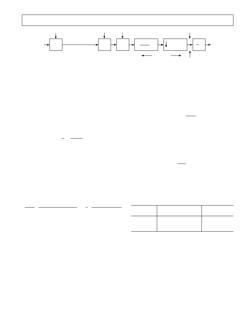
The operation of the AUX channel is identical to the Main
channel with the exception that there is no PGA on the AUX
channel. The input chopping is incorporated into the input
multiplexer while the output chopping is accomplished by an
XOR gate at the output of the modulator. The chopped modu-
lator bit stream is applied to a Sinc
3
filter. The programming of
the Sinc
3
decimation factor is restricted to an 8-bit register SF,
the actual decimation factor is the register value times 8. The
decimated output rate from the Sinc
3
filter (and the ADC con-
version rate) will therefore be:
f
SF
f
ADC
MOD
=
×
×
×
1
3
1
8
where
f
ADC
is the ADC update rate.
SF
is the decimal equivalent of the word loaded to the
filter register.
f
MOD
is the modulator sampling rate of 32.768 kHz.
Programming the filter register determines the update rate for
both the main and aux ADC. Both ADCs operate with the same
update rate.
The chop rate of the channel is half the output data rate.
The frequency response of the filter H (f) is as follows:
where
f
MOD
= 32,768 Hz
SF
= value programmed into SF SFR.
f
OUT
= f
MOD
/(SF
×
8
×
3)
The following shows plots of the filter frequency response for
the SF words shown in Table I. The overall frequency response
is the product of a Sinc
3
and a sinc response. There are Sinc
3
notches at integer multiples of 3
×
f
ADC
and there are sinc notches
1
8
8
1
2
2
3
SF
SF
sin(
f f
/
f f
/
f f
/
/
f f
MOD
)
MOD
OUT
OUT
×
×
×
×
×
×
×
×
×
π
×
×
sin(
)
sin(
sin(
)
)
π
π
π
SINC
3
FILTER
MUX
S-D
MOD1
XOR
ANALOG
INPUT
DIGITAL
OUTPUT
(8
SF
)
3
1
2
A
IN
+ V
OS
A
IN
–
V
OS
f
CHOP
f
MOD
f
CHOP
f
ADC
1
8
SF
3
(
)
Figure 5. Auxiliary ADC Channel Block Diagram
at odd integer multiples of f
ADC
/2. The 3 dB frequency for all
values of SF obeys the following equation:
f
(3
dB
) = 0.24
×
f
ADC
The signal chain is chopped as shown in Figures 4 and 5. The
chop frequency is:
f
f
CHOP
ADC
2
=
As shown in the block diagram, the Sinc
3
filter outputs alternately
contain +V
OS
and
–
V
OS
, where V
OS
is the respective channel
offset. This offset is removed by performing a running average
of 2. This average by 2 means that the settling time to any change
in programming of the ADC will be twice the normal conversion
time, while an asynchronous step change on the analog input will
not be fully reflected until the third subsequent output.
t
f
t
SETTLE
ADC
ADC
=
=
×
2
2
The allowable range for SF is 13 to 255, with a default of 69
(45H). The corresponding conversion rates, conversion times
and settling times are tabulated in Table I. Note that the con-
version time increases by 0.732 ms for each increment in SF.
Table I. ADC Conversion and Settling Times for Various
SF Words
SF
Word
Data Update Rate
f
ADC
(Hz)
105.3
19.79
5.35
Settling Time
t
SETTLE
(ms)
19.04
101.07
373.54
13
69 (Default)
255
Normal-mode rejection is the major function of the digital filter
on the AD7719. The normal mode 50
±
1 Hz rejection with an SF
word of 82 is typically
–
100 dB. The 60
±
1 Hz rejection with
SF = 68 is typically
–
100 dB. Simultaneous 50 Hz and 60 Hz
rejection of better than 60 dB is achieved with an SF of 69.
Choosing an SF word of 69 places notches at both 50 Hz and
60 Hz. Figures 6 to 9 show the filter rejection for a selection
of SF words.
相關PDF資料 |
PDF描述 |
|---|---|
| AD7720 | CMOS Sigma-Delta Modulator |
| AD7720BRU | CMOS Sigma-Delta Modulator |
| AD7721 | CMOS 16-Bit, 468.75 kHz, Sigma-Delta ADC |
| AD7721AN | CMOS 16-Bit, 468.75 kHz, Sigma-Delta ADC |
| AD7721AR | CMOS 16-Bit, 468.75 kHz, Sigma-Delta ADC |
相關代理商/技術參數 |
參數描述 |
|---|---|
| AD7719BR-REEL | 功能描述:IC ADC 16BIT 24BIT DUAL 28-SOIC RoHS:否 類別:集成電路 (IC) >> 數據采集 - 模數轉換器 系列:- 標準包裝:1,000 系列:- 位數:12 采樣率(每秒):300k 數據接口:并聯 轉換器數目:1 功率耗散(最大):75mW 電壓電源:單電源 工作溫度:0°C ~ 70°C 安裝類型:表面貼裝 封裝/外殼:24-SOIC(0.295",7.50mm 寬) 供應商設備封裝:24-SOIC 包裝:帶卷 (TR) 輸入數目和類型:1 個單端,單極;1 個單端,雙極 |
| AD7719BR-REEL7 | 功能描述:IC ADC 16BIT 24BIT DUAL 28-SOIC RoHS:否 類別:集成電路 (IC) >> 數據采集 - 模數轉換器 系列:- 標準包裝:1,000 系列:- 位數:12 采樣率(每秒):300k 數據接口:并聯 轉換器數目:1 功率耗散(最大):75mW 電壓電源:單電源 工作溫度:0°C ~ 70°C 安裝類型:表面貼裝 封裝/外殼:24-SOIC(0.295",7.50mm 寬) 供應商設備封裝:24-SOIC 包裝:帶卷 (TR) 輸入數目和類型:1 個單端,單極;1 個單端,雙極 |
| AD7719BRU | 制造商:Analog Devices 功能描述:ADC Dual Delta-Sigma 105sps 24-bit Serial 28-Pin TSSOP |
| AD7719BRU-REEL | 制造商:Analog Devices 功能描述:ADC Dual Delta-Sigma 105sps 24-bit Serial 28-Pin TSSOP T/R 制造商:Analog Devices 功能描述:ADC DUAL DELTA-SIGMA 0.105KSPS 24BIT SERL 28TSSOP - Tape and Reel |
| AD7719BRU-REEL7 | 制造商:Analog Devices 功能描述:ADC Dual Delta-Sigma 105sps 24-bit Serial 28-Pin TSSOP T/R |
發布緊急采購,3分鐘左右您將得到回復。