- 您現(xiàn)在的位置:買(mǎi)賣(mài)IC網(wǎng) > PDF目錄373915 > AD7719BR (ANALOG DEVICES INC) Low Voltage, Low Power, Factory-Calibrated 16-/24-Bit Dual ADC PDF資料下載
參數(shù)資料
| 型號(hào): | AD7719BR |
| 廠商: | ANALOG DEVICES INC |
| 元件分類(lèi): | ADC |
| 英文描述: | Low Voltage, Low Power, Factory-Calibrated 16-/24-Bit Dual ADC |
| 中文描述: | 6-CH 24-BIT DELTA-SIGMA ADC, SERIAL ACCESS, PDSO28 |
| 封裝: | MS-013AE, SOIC-28 |
| 文件頁(yè)數(shù): | 8/40頁(yè) |
| 文件大小: | 367K |
| 代理商: | AD7719BR |
第1頁(yè)第2頁(yè)第3頁(yè)第4頁(yè)第5頁(yè)第6頁(yè)第7頁(yè)當(dāng)前第8頁(yè)第9頁(yè)第10頁(yè)第11頁(yè)第12頁(yè)第13頁(yè)第14頁(yè)第15頁(yè)第16頁(yè)第17頁(yè)第18頁(yè)第19頁(yè)第20頁(yè)第21頁(yè)第22頁(yè)第23頁(yè)第24頁(yè)第25頁(yè)第26頁(yè)第27頁(yè)第28頁(yè)第29頁(yè)第30頁(yè)第31頁(yè)第32頁(yè)第33頁(yè)第34頁(yè)第35頁(yè)第36頁(yè)第37頁(yè)第38頁(yè)第39頁(yè)第40頁(yè)
REV. 0
AD7719
–8–
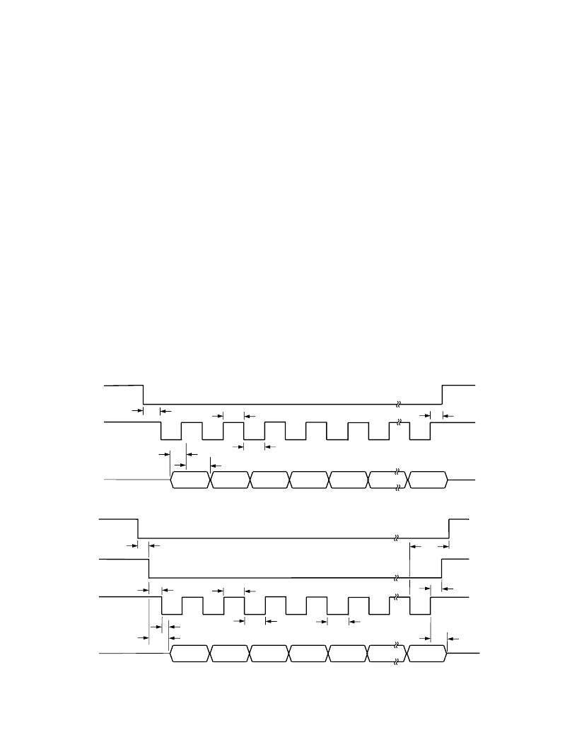
t
12
t
13
t
14
t
15
t
11
t
16
MSB
LSB
CS
SCLK
DIN
Figure 2. Write Cycle Timing Diagram
t
5
t
5A
t
4
t
6
t
3
t
9
MSB
LSB
CS
SCLK
t
8
t
10
t
7
t
6
DOUT
RDY
Figure 3. Read Cycle Timing Diagram
to ensure that a data read is not attempted while the register is
being updated.
CS
is used to select the device. It can be used to
decode the AD7719 in systems where a number of parts are
connected to the serial bus.
Figures 2 and 3 show timing diagrams for interfacing to the
AD7719 with
CS
used to decode the part. Figure 3 is for a read
operation from the AD7719
’
s output shift register while Figure 2
shows a write operation to the input shift register. It is possible
to read the same data twice from the output register even though
the
RDY
line returns high after the first read operation. Care must
be taken, however, to ensure that the read operations have been
completed before the next output update is about to take place.
The AD7719 serial interface can operate in 3-wire mode by
tying the
CS
input low. In this case, the SCLK, DIN, and
DOUT lines are used to communicate with the AD7719 and
the status of RDY bits (RDY0 and RDY1) can be obtained by
interrogating the STATUS Register. This scheme is suitable
for interfacing to microcontrollers. If
CS
is required as a decod-
ing signal, it can be generated from a port bit. For microcontroller
interfaces, it is recommended that the SCLK idles high between
data transfers.
The AD7719 can also be operated with
CS
used as a frame
synchronization signal. This scheme is suitable for DSP inter-
faces. In this case, the first bit (MSB) is effectively clocked out
by
CS
since
CS
would normally occur after the falling edge of
SCLK in DSPs. The SCLK can continue to run between data
transfers provided the timing numbers are obeyed.
DIGITAL INTERFACE
As previously outlined, the AD7719
’
s programmable functions
are controlled using a set of on-chip registers. Data is written to
these registers via the part
’
s serial interface and read access to
the on-chip registers is also provided by this interface. All com-
munications to the part must start with a write operation to the
Communications Register. After power-on or
RESET
, the device
expects a write to its Communications Register. The data writ-
ten to this register determines whether the next operation to the
part is a read or a write operation and also determines to which
register this read or write operation occurs. Therefore, write
access to any of the other registers on the part starts with a write
operation to the Communications Register followed by a write
to the selected register. A read operation from any other register
on the part (including the output data register) starts with a
write operation to the Communications Register followed by a
read operation from the selected register.
The AD7719
’
s serial interface consists of five signals,
CS
, SCLK,
DIN, DOUT, and
RDY
. The DIN line is used for transferring
data into the on-chip registers while the DOUT line is used for
accessing data from the on-chip registers. SCLK is the serial
clock input for the device and all data transfers (either on DIN
or DOUT) take place with respect to this SCLK signal. The
RDY
line is used as a status signal to indicate when data is ready
to be read from the AD7719
’
s data register.
RDY
goes low when a
new data word is available in the output register of either the
main or Aux ADCs. It is reset high when a read operation from
the data register is complete. It also goes high prior to the updating
of the output register to indicate when
not
to read from the device
相關(guān)PDF資料 |
PDF描述 |
|---|---|
| AD7720 | CMOS Sigma-Delta Modulator |
| AD7720BRU | CMOS Sigma-Delta Modulator |
| AD7721 | CMOS 16-Bit, 468.75 kHz, Sigma-Delta ADC |
| AD7721AN | CMOS 16-Bit, 468.75 kHz, Sigma-Delta ADC |
| AD7721AR | CMOS 16-Bit, 468.75 kHz, Sigma-Delta ADC |
相關(guān)代理商/技術(shù)參數(shù) |
參數(shù)描述 |
|---|---|
| AD7719BR-REEL | 功能描述:IC ADC 16BIT 24BIT DUAL 28-SOIC RoHS:否 類(lèi)別:集成電路 (IC) >> 數(shù)據(jù)采集 - 模數(shù)轉(zhuǎn)換器 系列:- 標(biāo)準(zhǔn)包裝:1,000 系列:- 位數(shù):12 采樣率(每秒):300k 數(shù)據(jù)接口:并聯(lián) 轉(zhuǎn)換器數(shù)目:1 功率耗散(最大):75mW 電壓電源:單電源 工作溫度:0°C ~ 70°C 安裝類(lèi)型:表面貼裝 封裝/外殼:24-SOIC(0.295",7.50mm 寬) 供應(yīng)商設(shè)備封裝:24-SOIC 包裝:帶卷 (TR) 輸入數(shù)目和類(lèi)型:1 個(gè)單端,單極;1 個(gè)單端,雙極 |
| AD7719BR-REEL7 | 功能描述:IC ADC 16BIT 24BIT DUAL 28-SOIC RoHS:否 類(lèi)別:集成電路 (IC) >> 數(shù)據(jù)采集 - 模數(shù)轉(zhuǎn)換器 系列:- 標(biāo)準(zhǔn)包裝:1,000 系列:- 位數(shù):12 采樣率(每秒):300k 數(shù)據(jù)接口:并聯(lián) 轉(zhuǎn)換器數(shù)目:1 功率耗散(最大):75mW 電壓電源:單電源 工作溫度:0°C ~ 70°C 安裝類(lèi)型:表面貼裝 封裝/外殼:24-SOIC(0.295",7.50mm 寬) 供應(yīng)商設(shè)備封裝:24-SOIC 包裝:帶卷 (TR) 輸入數(shù)目和類(lèi)型:1 個(gè)單端,單極;1 個(gè)單端,雙極 |
| AD7719BRU | 制造商:Analog Devices 功能描述:ADC Dual Delta-Sigma 105sps 24-bit Serial 28-Pin TSSOP |
| AD7719BRU-REEL | 制造商:Analog Devices 功能描述:ADC Dual Delta-Sigma 105sps 24-bit Serial 28-Pin TSSOP T/R 制造商:Analog Devices 功能描述:ADC DUAL DELTA-SIGMA 0.105KSPS 24BIT SERL 28TSSOP - Tape and Reel |
| AD7719BRU-REEL7 | 制造商:Analog Devices 功能描述:ADC Dual Delta-Sigma 105sps 24-bit Serial 28-Pin TSSOP T/R |
發(fā)布緊急采購(gòu),3分鐘左右您將得到回復(fù)。