- 您現在的位置:買賣IC網 > PDF目錄373916 > AD7742BR (ANALOG DEVICES INC) Single and Multichannel, Synchronous Voltage-to-Frequency Converters PDF資料下載
參數資料
| 型號: | AD7742BR |
| 廠商: | ANALOG DEVICES INC |
| 元件分類: | 模擬專用變換器 |
| 英文描述: | Single and Multichannel, Synchronous Voltage-to-Frequency Converters |
| 中文描述: | VOLTAGE-FREQUENCY CONVERTER, 6.144 MHz, PDSO16 |
| 封裝: | SOIC-16 |
| 文件頁數: | 10/12頁 |
| 文件大小: | 131K |
| 代理商: | AD7742BR |
REV. 0
AD7741/AD7742
–10–
APPLICATIONS
The basic connection diagram for the part is shown in Figure 9.
In the connection diagram shown, the AD7742 analog inputs
are configured as fully differential, bipolar inputs with a gain of
1. A quartz crystal provides the master clock source for the part.
It may be necessary to connect capacitors (C1 and C2 in the
diagram) on the crystal to ensure that it does not oscillate at over-
tones of its fundamental operating frequency. The values of ca-
pacitors will vary depending on the manufacturer’s specifications.
CLKOUT
CLKIN
REFIN
f
OUT
GND
UNI/
BIP
GAIN
C1
C2
DIFF
INPUT 1
DIFF
INPUT 2
CHANNEL
SELECT
V
IN
1
V
IN
2
V
IN
3
V
IN
4
A0
A1
V
DD
PD
AD7742
+5V
REFOUT
Figure 9. Basic Connection Diagram
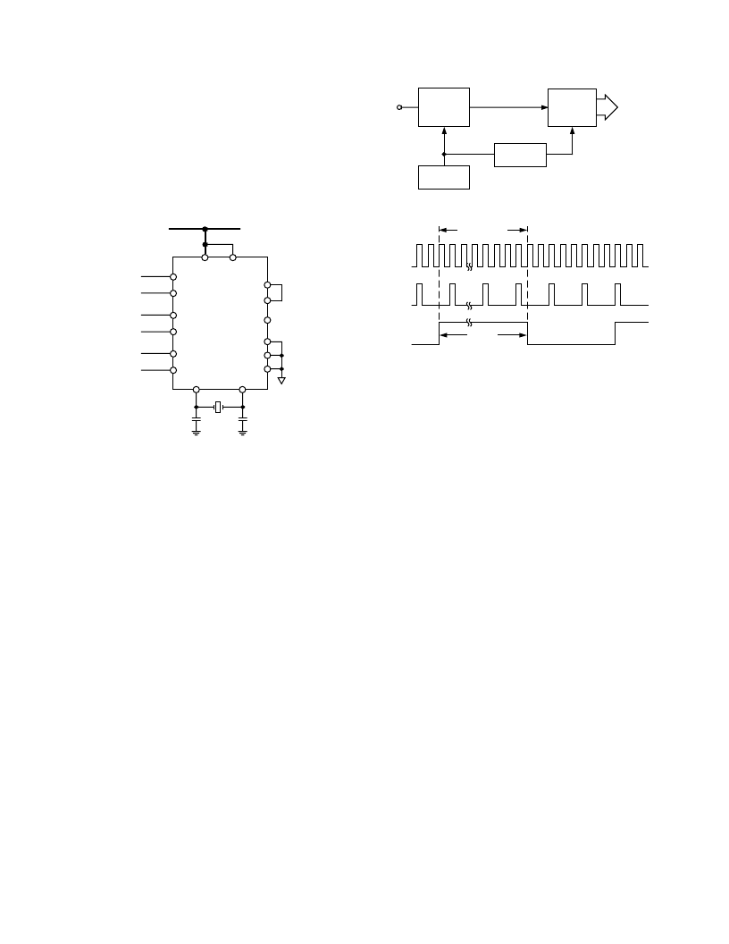
A/D Conversion Techniques Using the AD7741/AD7742
When used as an ADC, VFCs provide certain advantages in-
cluding accuracy, linearity and being inherently monotonic. The
AD7741/AD7742 has a true integrating input which smooths
out noise peaks.
The most popular method of using a VFC in an A/D system is
to count the output pulses of f
OUT
for a fixed gate interval (see
Figure 10). This fixed gate interval should be generated by
dividing down the clock input frequency. This ensures that any
errors due to clock jitter or clock frequency drift are eliminated.
The ratio of the f
OUT
to the clock frequency is what is important
here, not the absolute value of f
OUT
. The frequency division can
be done by a binary counter where f
CLKIN
is the CLK input.
Figure 11 shows the waveforms of f
CLKIN
, f
OUT
and the Gate
signal. A counter counts the rising edges of f
OUT
while the Gate
signal is high. Since the gate interval is not synchronized with
f
OUT
, there is a possibility of a counting inaccuracy. Depending
on f
OUT,
an error of one count may occur.
COUNTER
AD7741
f
OUT
V
IN
CLOCK
GENERATOR
GATE
SIGNAL
TO
m
P
CLKIN
FREQUENCY
DIVIDER
Figure 10. A/D Conversion Using the AD7741 VFC
f
CLKIN
f
OUT
GATE
T
GATE
4096x T
CLOCK
Figure 11. Waveforms in an A/D Converter Using a VFC
The clock frequency and the gate time determine the resolution
of such an ADC. If 12-bit resolution is required and f
CLKIN
is
5 MHz (therefore, f
OUT
max is 2.25 MHz), the minimum gate
time required is calculated as follows:
N counts at Full Scale (2.25 MHz) will take
(
N
/2.25
×
10
6
)
seconds
=
minimum gate time.
N
is the total number of codes for a given resolution; 4096 for
12 bits
minimum gate time =
(4096/2.25
×
10
6
)
sec =
1.820
ms.
Since T
GATE
×
f
OUT
max = number of counts at full scale, a
faster conversion with the same resolution can be performed
with a higher f
OUT
max. This high f
OUT
max (3 MHz) is a main
feature of the AD7741/AD7742.
If the output frequency is measured by counting pulses gated to
a signal which is derived from the clock, the clock stability is
unimportant and the device simply performs as a voltage-
controlled frequency divider, producing a high resolution ADC.
The inherent monotonicity of the transfer function and wide
range of input clock frequencies allows the conversion time and
resolution to be optimized for specific applications.
There is another parameter is taken into account when choosing
the length of the gate interval. Because the integration period of
the system is equal to the gate interval, any interfering signal can
be rejected by counting for an integer number of periods of the
interfering signal. For example, a gate interval of 100 ms will
give normal-mode rejection of 50 Hz and 60 Hz signals.
相關PDF資料 |
PDF描述 |
|---|---|
| AD774BJR | Complete 12-Bit A/D Converters |
| AD774BAR | Complete 12-Bit A/D Converters |
| AD774BBR | Complete 12-Bit A/D Converters |
| AD774BAD | Complete 12-Bit A/D Converters |
| AD774BBD | Complete 12-Bit A/D Converters |
相關代理商/技術參數 |
參數描述 |
|---|---|
| AD7742BR-REEL | 制造商:Analog Devices 功能描述: |
| AD7742YR | 制造商:AD 制造商全稱:Analog Devices 功能描述:Single and Multichannel, Synchronous Voltage-to-Frequency Converters |
| AD7742YR-REEL | 制造商:Analog Devices 功能描述: |
| AD7742YR-REEL7 | 制造商:Analog Devices 功能描述: |
| AD7742YRZ | 制造商:Analog Devices 功能描述:VFC Sync 2.75MHz 16-Pin SOIC N |
發布緊急采購,3分鐘左右您將得到回復。