- 您現(xiàn)在的位置:買賣IC網(wǎng) > PDF目錄373916 > AD7742BR (ANALOG DEVICES INC) Single and Multichannel, Synchronous Voltage-to-Frequency Converters PDF資料下載
參數(shù)資料
| 型號: | AD7742BR |
| 廠商: | ANALOG DEVICES INC |
| 元件分類: | 模擬專用變換器 |
| 英文描述: | Single and Multichannel, Synchronous Voltage-to-Frequency Converters |
| 中文描述: | VOLTAGE-FREQUENCY CONVERTER, 6.144 MHz, PDSO16 |
| 封裝: | SOIC-16 |
| 文件頁數(shù): | 8/12頁 |
| 文件大小: | 131K |
| 代理商: | AD7742BR |
REV. 0
AD7741/AD7742
–8–
As can be seen from Table II, the AD7741 has one input range
configuration whereas the AD7742 has unipolar/bipolar as
well as gain options depending on the status of the GAIN
and UNI/
BIP
pins.
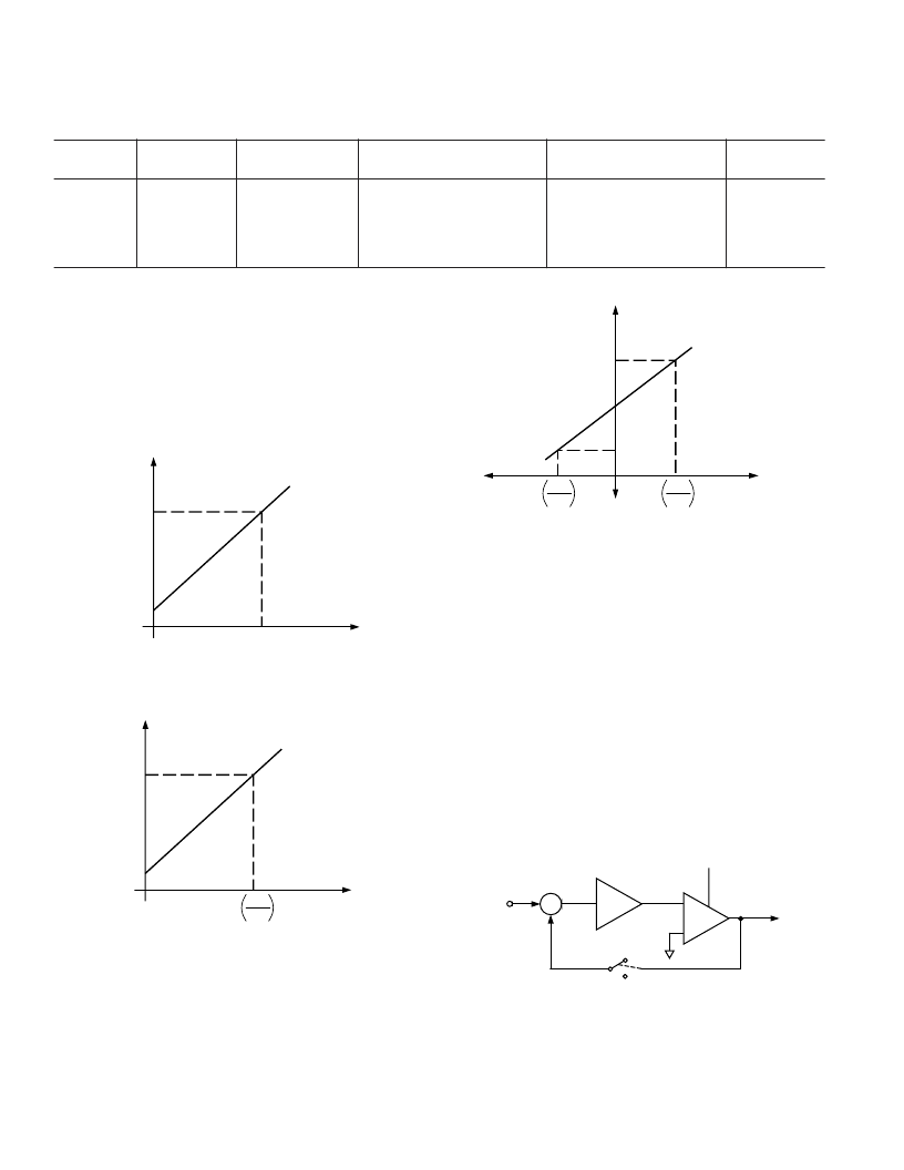
The transfer function for the AD7741 is shown in Figure 3.
Figure 4 shows the AD7742 transfer function for unipolar input
range configuration while the AD7742 transfer function for
bipolar input range configuration is shown in Figure 5.
OUTPUT
FREQUENCY
f
OUT
f
OUT
MAX
(0.45 f
CLKIN
)
f
OUT
MIN
(0.05 f
CLKIN
)
0
INPUT
VOLTAGE V
IN
REFIN
Figure 3. AD7741 Transfer Characteristic for Input Range
from 0 to V
REF
OUTPUT
FREQUENCY
f
OUT
f
OUT
MAX
(0.45 f
CLKIN
)
f
OUT
MIN
(0.05 f
CLKIN
)
0
V
REF
GAIN
+
DIFFERENTIAL
INPUT VOLTAGE
Figure 4. AD7742 Transfer Characteristic for Unipolar
Differential Input Range: 0 V to V
REF
/Gain; the input
common-mode range must be between +0.5 V and
V
DD
– 1.75 V. UNI/
BIP
pin tied to V
DD
.
Table II. AD7741/AD7742 Input Range Selection
V
IN
(Min)
f
OUT
= 0.05 f
CLKIN
0
–V
REF
–V
REF
/2
0
0
V
IN
(Max)
f
OUT
= 0.45 f
CLKIN
+V
REF
+V
REF
+V
REF
/2
+V
REF
+V
REF
/2
UNI/
BIP
GAIN
Gain, G
Part
N/A
0
0
1
1
N/A
0
1
0
1
X1
X1
X2
X1
X2
AD7741
AD7742
AD7742
AD7742
AD7742
OUTPUT
FREQUENCY
f
OUT
f
OUT
MAX
(0.45 f
CLKIN
)
f
OUT
MIN
(0.05 f
CLKIN
)
DIFFERENTIAL
INPUT VOLTAGE
V
REF
GAIN
+
V
REF
GAIN
–
Figure 5. AD7742 Transfer Characteristic for Bipolar
Differential Input Range: –V
REF
/Gain to +V
REF
/Gain; the
common-mode range must be between +0.5 V and
V
DD
– 1.75 V. UNI/
BIP
pin tied to GND.
VFC Modulator
The analog input signal to the AD7741/AD7742 is continu-
ously sampled by a switched capacitor modulator whose sam-
pling rate is set by a master clock input that may be supplied
externally or by a crystal-controlled on-chip clock oscillator.
However, the input signal is buffered on-chip before being ap-
plied to the sampling capacitor of the modulator. This isolates
the sampling capacitor charging currents from the analog input
pins.
This system is a negative feedback loop that tries to keep the net
charge on the integrator capacitor at zero, by balancing charge
injected by the input voltage with charge injected by the V
REF
.
The output of the comparator provides the digital input for the
1-bit DAC, so that the system functions as a negative feedback
loop that tries to minimize the difference signal (see Figure 6).
INTEGRATOR
COMPARATOR
+
–
CLK
1-BIT
STREAM
+
S
INPUT
+V
REF
–V
REF
–
Figure 6. AD7741/AD7742 Modulator Loop
相關(guān)PDF資料 |
PDF描述 |
|---|---|
| AD774BJR | Complete 12-Bit A/D Converters |
| AD774BAR | Complete 12-Bit A/D Converters |
| AD774BBR | Complete 12-Bit A/D Converters |
| AD774BAD | Complete 12-Bit A/D Converters |
| AD774BBD | Complete 12-Bit A/D Converters |
相關(guān)代理商/技術(shù)參數(shù) |
參數(shù)描述 |
|---|---|
| AD7742BR-REEL | 制造商:Analog Devices 功能描述: |
| AD7742YR | 制造商:AD 制造商全稱:Analog Devices 功能描述:Single and Multichannel, Synchronous Voltage-to-Frequency Converters |
| AD7742YR-REEL | 制造商:Analog Devices 功能描述: |
| AD7742YR-REEL7 | 制造商:Analog Devices 功能描述: |
| AD7742YRZ | 制造商:Analog Devices 功能描述:VFC Sync 2.75MHz 16-Pin SOIC N |
發(fā)布緊急采購,3分鐘左右您將得到回復(fù)。