- 您現(xiàn)在的位置:買賣IC網(wǎng) > PDF目錄373916 > AD7742BR (ANALOG DEVICES INC) Single and Multichannel, Synchronous Voltage-to-Frequency Converters PDF資料下載
參數(shù)資料
| 型號(hào): | AD7742BR |
| 廠商: | ANALOG DEVICES INC |
| 元件分類: | 模擬專用變換器 |
| 英文描述: | Single and Multichannel, Synchronous Voltage-to-Frequency Converters |
| 中文描述: | VOLTAGE-FREQUENCY CONVERTER, 6.144 MHz, PDSO16 |
| 封裝: | SOIC-16 |
| 文件頁數(shù): | 4/12頁 |
| 文件大小: | 131K |
| 代理商: | AD7742BR |
REV. 0
AD7741/AD7742
–4–
CAUTION
ESD (electrostatic discharge) sensitive device. Electrostatic charges as high as 4000 V readily
accumulate on the human body and test equipment and can discharge without detection.
Although the AD7741/AD7742 features proprietary ESD protection circuitry, permanent dam-
age may occur on devices subjected to high energy electrostatic discharges. Therefore, proper
ESD precautions are recommended to avoid performance degradation or loss of functionality.
WARNING!
ESD SENSITIVE DEVICE
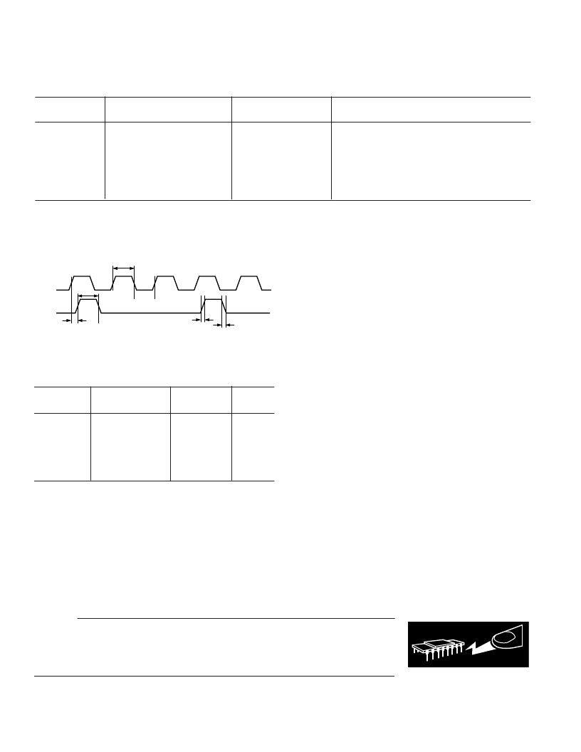
TIMING CHARACTERISTICS
1, 2, 3
Limit at T
MIN
, T
MAX
(B and Y Version)
Parameter
Units
Conditions/Comments
f
CLKIN
t
HIGH
/t
LOW
6.144
55/45
45/55
9
4
4
t
HIGH
±
5
MHz max
max
min
ns typ
ns typ
ns typ
ns typ
Input Clock Mark/Space Ratio
t
1
t
2
t
3
t
4
f
CLOCK
Rising Edge to f
OUT
Rising Edge
f
OUT
Rise Time
f
OUT
Fall Time
f
OUT
Pulsewidth
NOTES
1
Guaranteed by design and characterization, not production tested.
2
All input signals are specified with tr = tf = 5 ns (10% to 90% of V
DD
) and timed from a voltage level of (V
IL
+ V
IH
)/2.
3
See Figure 1.
Specifications subject to change without notice.
(V
DD
= +4.75 V to +5.25 V; V
REF
= +2.5 V. All specifications T
MIN
to T
MAX
unless otherwise noted.)
ABSOLUTE MAXIMUM RATINGS
1, 2
(T
A
= +25
°
C unless otherwise noted)
V
DD
to GND . . . . . . . . . . . . . . . . . . . . . . . . . . –0.3V to +7 V
Analog Input Voltage to GND . . . . . . . . –5V to V
DD
+ 0.3 V
Digital Input Voltage to GND . . . . . . . –0.3V to V
DD
+ 0.3 V
Reference Input Voltage to GND . . . . –0.3 V to V
DD
+ 0.3 V
f
OUT
to GND . . . . . . . . . . . . . . . . . . . . –0.3 V to V
DD
+ 0.3 V
Operating Temperature Range
Automotive (Y Version) . . . . . . . . . . . . . . –40
°
C to +105
°
C
Industrial (B Version) . . . . . . . . . . . . . . . . –40
°
C to +85
°
C
Storage Temperature Range . . . . . . . . . . . . –65
°
C to +150
°
C
Junction Temperature . . . . . . . . . . . . . . . . . . . . . . . . +150
°
C
Plastic DIP Package
Power Dissipation . . . . . . . . . . . . . . . . . . . . . . . . . 450 mW
θ
JA
Thermal Impedance (8 Lead) . . . . . . . . . . . . . 125
°
C/W
θ
JA
Thermal Impedance (16 Lead) . . . . . . . . . . . . 117
°
C/W
Lead Temperature, Soldering
Vapor Phase (60 sec) . . . . . . . . . . . . . . . . . . . . . +215
°
C
Infrared (15 sec) . . . . . . . . . . . . . . . . . . . . . . . . . +220
°
C
SOIC Package
Power Dissipation . . . . . . . . . . . . . . . . . . . . . . . . . 450 mW
θ
JA
Thermal Impedance (8 Lead) . . . . . . . . . . . . . 157
°
C/W
θ
JA
Thermal Impedance (16 Lead) . . . . . . . . . . . . 125
°
C/W
Lead Temperature, Soldering
Vapor Phase (60 sec) . . . . . . . . . . . . . . . . . . . . . +215
°
C
Infrared (15 sec) . . . . . . . . . . . . . . . . . . . . . . . . . +220
°
C
NOTES
1
Stresses above those listed under Absolute Maximum Ratings may cause perma-
nent damage to the device. This is a stress rating only; functional operation of the
device at these or any other conditions above those listed in the operational
sections of this specification is not implied. Exposure to absolute maximum rating
conditions for extended periods may affect device reliability.
2
Transient currents of up to 100 mA will not cause SCR latch-up.
ORDERING GUIDE
Temperature
Ranges
Package
Descriptions
Package
Options
Models
AD7741BN
AD7741BR
AD7741YR
AD7742BN
AD7742BR
AD7742YR
–40
°
C to +85
°
C
–40
°
C to +85
°
C
–40
°
C to +105
°
C
–40
°
C to +85
°
C
–40
°
C to +85
°
C
–40
°
C to +105
°
C
Plastic DIP
Small Outline
Small Outline
Plastic DIP
Small Outline
Small Outline
N-8
R-8
R-8
N-16
R-16A
R-16A
CLKIN
f
OUT
t
HIGH
t
4
t
1
t
2
t
3
Figure 1. Timing Diagram
相關(guān)PDF資料 |
PDF描述 |
|---|---|
| AD774BJR | Complete 12-Bit A/D Converters |
| AD774BAR | Complete 12-Bit A/D Converters |
| AD774BBR | Complete 12-Bit A/D Converters |
| AD774BAD | Complete 12-Bit A/D Converters |
| AD774BBD | Complete 12-Bit A/D Converters |
相關(guān)代理商/技術(shù)參數(shù) |
參數(shù)描述 |
|---|---|
| AD7742BR-REEL | 制造商:Analog Devices 功能描述: |
| AD7742YR | 制造商:AD 制造商全稱:Analog Devices 功能描述:Single and Multichannel, Synchronous Voltage-to-Frequency Converters |
| AD7742YR-REEL | 制造商:Analog Devices 功能描述: |
| AD7742YR-REEL7 | 制造商:Analog Devices 功能描述: |
| AD7742YRZ | 制造商:Analog Devices 功能描述:VFC Sync 2.75MHz 16-Pin SOIC N |
發(fā)布緊急采購,3分鐘左右您將得到回復(fù)。