- 您現(xiàn)在的位置:買賣IC網(wǎng) > PDF目錄373920 > AD7854 (Analog Devices, Inc.) 12-Bit Sampling ADC(單電源,200kSPS 12位采樣A/D轉(zhuǎn)換器) PDF資料下載
參數(shù)資料
| 型號: | AD7854 |
| 廠商: | Analog Devices, Inc. |
| 英文描述: | 12-Bit Sampling ADC(單電源,200kSPS 12位采樣A/D轉(zhuǎn)換器) |
| 中文描述: | 12位采樣ADC(單電源,速度高達200ksps的12位采樣的A / D轉(zhuǎn)換器) |
| 文件頁數(shù): | 8/28頁 |
| 文件大小: | 268K |
| 代理商: | AD7854 |
第1頁第2頁第3頁第4頁第5頁第6頁第7頁當前第8頁第9頁第10頁第11頁第12頁第13頁第14頁第15頁第16頁第17頁第18頁第19頁第20頁第21頁第22頁第23頁第24頁第25頁第26頁第27頁第28頁
AD7854/AD7854L
–8–
REV. 0
AD7854/AD7854L ON-CHIP RE GIST E RS
T he AD7854/AD7854L powers up with a set of default conditions, and the user need not ever write to the device. In this case the
AD7854/AD7854L will operate as a read-only ADC. T he
WR
pin should be tied to DV
DD
for operating the AD7854/AD7854L as a
read-only ADC.
Extra features and flexibility such as performing different power-down options, different types of calibrations including system cali-
bration, and software conversion start can be selected by writing to the part.
T he AD7854/AD7854L contains a
control register, ADC output data register, status register, test register
and
10 calibra-
tion registers
. T he control register is write-only, the ADC output data register and the status register are read-only, and the test and
calibration registers are both read/write registers. T he test register is used for testing the part and should not be written to.
Addressing the On-Chip Registers
Writing
T o write to the AD7854/AD7854L, a 16-bit word of data must be transferred. T his transfer consists of two 8-bit writes. T he first
8 bits of data that are written
must
consist of the 8 LSBs of the 16-bit word and the second 8 bits that are written
must
consist of the
8 MSBs of the 16-bit word. For each of these 8-bit writes, the data is placed on Pins DB0 to DB7, Pin DB0 being the LSB of each
transfer and Pin DB7 being the MSB of each transfer. T he two MSBs of the 16-bit word, ADDR1 and ADDR0, are decoded to de-
termine which register is addressed, and the 14 LSBs are written to the addressed register. T able I shows the decoding of the address
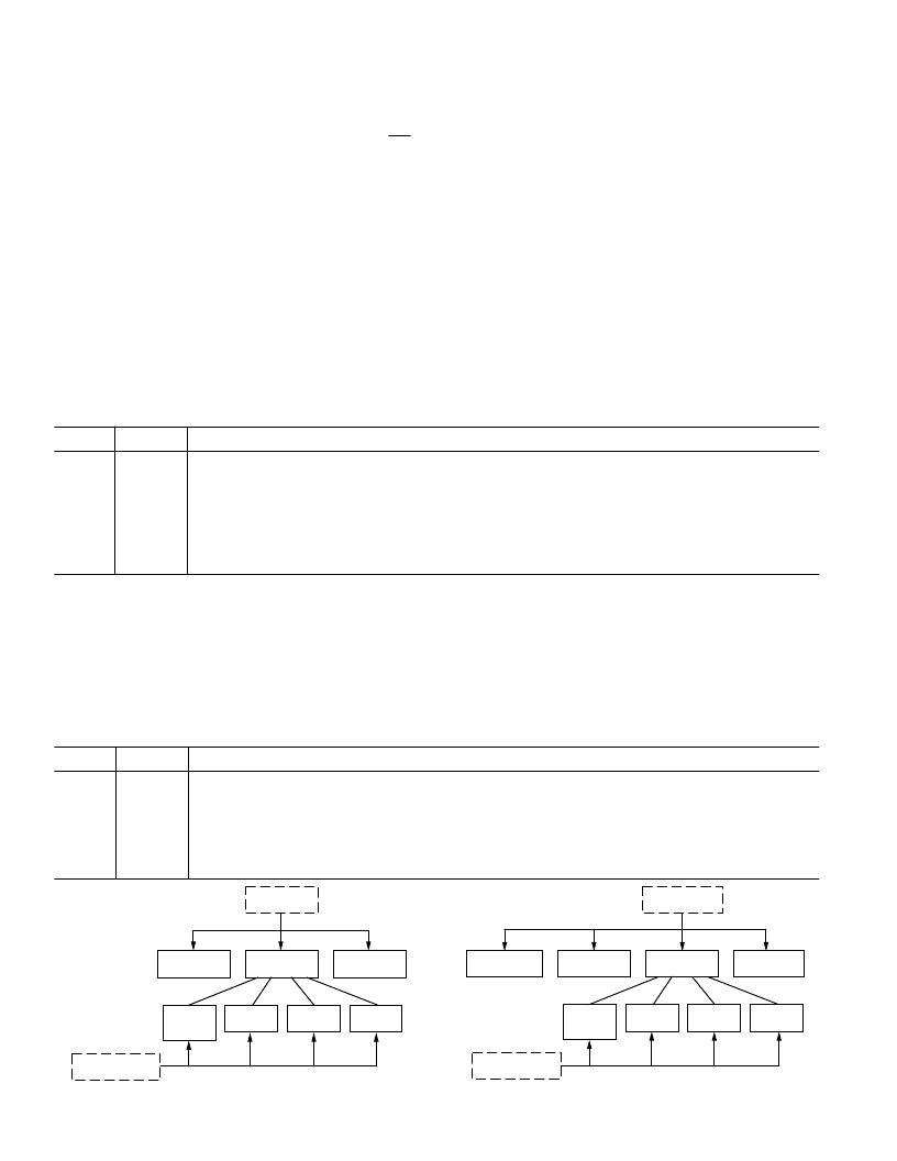
bits, while Figure 2 shows the overall write register hierarchy.
T able I. Write Register Addressing
ADDR1
ADDR0
Comment
0
0
1
0
1
0
T his combination does not address any register.
T his combination addresses the
TE ST RE GISTE R
. T he 14 LSBs of data are written to the test register.
T his combination addresses the
CALIBRAT ION RE GIST E R
. T he 14 least significant data bits are writ-
ten to the selected calibration register.
T his combination addresses the
CONT ROL RE GIST E R
. T he 14 least significant data bits are written to
the control register.
1
1
Reading
T o read from the various registers the user must first write to Bits 6 and 7 in the Control Register, RDSLT 0 and RDSLT 1. T hese
bits are decoded to determine which register is addressed during a read operation. T able II shows the decoding of the read address
bits while Figure 3 shows the overall read register hierarchy. T he power-up status of these bits is 00 so that the default read will be
from the ADC output data register. Note: when reading from the calibration registers, the low byte must always be read first.
Once the read selection bits are set in the control register all subsequent read operations that follow are from the selected register
until the read selection bits are changed in the control register.
T able II. Read Register Addressing
RDSLT 1
RDSLT 0
Comment
0
0
All successive read operations are from the
ADC OUT PUT DAT A RE GIST E R
. T his is the default power-
up setting. T here is always four leading zeros when reading from the ADC output data register.
All successive read operations are from the
T E ST RE GIST E R
.
All successive read operations are from the
CALIBRAT ION RE GIST E RS
.
All successive read operations are from the
ST AT US RE GIST E R
.
0
1
1
1
0
1
TEST
REGISTER
CALIBRATION
REGISTERS
CONTROL
REGISTER
ADDR1, ADDR0
DECODE
01
10
11
GAIN(1)
OFFSET(1)
DAC(8)
GAIN(1)
OFFSET(1)
OFFSET(1)
GAIN(1)
CALSLT1, CALSLT0
DECODE
00
01
10
11
Figure 2. Write Register Hierarchy/Address Decoding
TEST
REGISTER
CALIBRATION
REGISTERS
CONTROL
REGISTER
RDSLT1, RDSLT0
DECODE
01
10
11
GAIN(1)
OFFSET(1)
DAC(8)
GAIN(1)
OFFSET(1)
OFFSET(1)
GAIN(1)
CALSLT1, CALSLT0
DECODE
00
01
10
11
ADC OUTPUT
DATA REGISTER
00
Figure 3. Read Register Hierarchy/Address Decoding
相關(guān)PDF資料 |
PDF描述 |
|---|---|
| AD7858LARS | 3 V to 5 V Single Supply, 200 kSPS 8-Channel, 12-Bit Sampling ADC |
| AD7858BN | 3 V to 5 V Single Supply, 200 kSPS 8-Channel, 12-Bit Sampling ADC |
| AD7858BR | 3 V to 5 V Single Supply, 200 kSPS 8-Channel, 12-Bit Sampling ADC |
| AD7858AN | 3 V to 5 V Single Supply, 200 kSPS 8-Channel, 12-Bit Sampling ADC |
| AD7858AR | 3 V to 5 V Single Supply, 200 kSPS 8-Channel, 12-Bit Sampling ADC |
相關(guān)代理商/技術(shù)參數(shù) |
參數(shù)描述 |
|---|---|
| AD7854AD | 制造商:Analog Devices 功能描述: |
| AD7854AQ | 功能描述:IC ADC 12BIT PARALLEL LP 28-CDIP RoHS:否 類別:集成電路 (IC) >> 數(shù)據(jù)采集 - 模數(shù)轉(zhuǎn)換器 系列:- 標準包裝:1,000 系列:- 位數(shù):12 采樣率(每秒):300k 數(shù)據(jù)接口:并聯(lián) 轉(zhuǎn)換器數(shù)目:1 功率耗散(最大):75mW 電壓電源:單電源 工作溫度:0°C ~ 70°C 安裝類型:表面貼裝 封裝/外殼:24-SOIC(0.295",7.50mm 寬) 供應商設備封裝:24-SOIC 包裝:帶卷 (TR) 輸入數(shù)目和類型:1 個單端,單極;1 個單端,雙極 |
| AD7854AR | 功能描述:IC ADC 12BIT PARALLEL LP 28-SOIC RoHS:否 類別:集成電路 (IC) >> 數(shù)據(jù)采集 - 模數(shù)轉(zhuǎn)換器 系列:- 標準包裝:1,000 系列:- 位數(shù):12 采樣率(每秒):300k 數(shù)據(jù)接口:并聯(lián) 轉(zhuǎn)換器數(shù)目:1 功率耗散(最大):75mW 電壓電源:單電源 工作溫度:0°C ~ 70°C 安裝類型:表面貼裝 封裝/外殼:24-SOIC(0.295",7.50mm 寬) 供應商設備封裝:24-SOIC 包裝:帶卷 (TR) 輸入數(shù)目和類型:1 個單端,單極;1 個單端,雙極 |
| AD7854AR-REEL | 制造商:Analog Devices 功能描述:ADC Single SAR 200ksps 12-bit Parallel 28-Pin SOIC W T/R 制造商:Analog Devices 功能描述:ADC SGL SAR 200KSPS 12-BIT PARALLEL 28SOIC W - Tape and Reel |
| AD7854ARS | 功能描述:IC ADC 12BIT PARALLEL LP 28-SSOP RoHS:否 類別:集成電路 (IC) >> 數(shù)據(jù)采集 - 模數(shù)轉(zhuǎn)換器 系列:- 標準包裝:1,000 系列:- 位數(shù):12 采樣率(每秒):300k 數(shù)據(jù)接口:并聯(lián) 轉(zhuǎn)換器數(shù)目:1 功率耗散(最大):75mW 電壓電源:單電源 工作溫度:0°C ~ 70°C 安裝類型:表面貼裝 封裝/外殼:24-SOIC(0.295",7.50mm 寬) 供應商設備封裝:24-SOIC 包裝:帶卷 (TR) 輸入數(shù)目和類型:1 個單端,單極;1 個單端,雙極 |
發(fā)布緊急采購,3分鐘左右您將得到回復。