- 您現在的位置:買賣IC網 > PDF目錄373921 > AD7865AS-1 (ANALOG DEVICES INC) Four-Channel, Simultaneous Sampling, Fast, 14-Bit ADC PDF資料下載
參數資料
| 型號: | AD7865AS-1 |
| 廠商: | ANALOG DEVICES INC |
| 元件分類: | ADC |
| 英文描述: | Four-Channel, Simultaneous Sampling, Fast, 14-Bit ADC |
| 中文描述: | 4-CH 14-BIT SUCCESSIVE APPROXIMATION ADC, PARALLEL ACCESS, PQFP44 |
| 封裝: | PLASTIC, QFP-44 |
| 文件頁數: | 13/19頁 |
| 文件大小: | 195K |
| 代理商: | AD7865AS-1 |
AD7865
–13–
REV. A
Accessing the Output Data Registers
There are four Output Data Registers, one for each of the four
possible conversion results from a conversion sequence. The
result of the first conversion in a conversion sequence is placed
in Register 1 and the second result is placed in Register 2 and
so on. For example if the conversion sequence V
IN1
, V
IN3
and
V
IN4
is selected (see Selecting a Conversion Sequence) the
results of the conversion on V
IN1
, V
IN3
and V
IN4
are placed in
Registers 1 to 3 respectively. The Output Data register pointer
is reset to point to Register 1 at the end of the first conversion
in the sequence, just prior to
EOC
going low. At this point the
logic output FRSTDATA will go logic high to indicate that the
output data register pointer is addressing Register 1. When
CS
and
RD
are both logic low the contents of the addressed regis-
ter are enabled onto the data bus (DB0–DB13).
DB0 TO
DB13
O/P
DRIVERS
OE
#1
NOT VALID
(V
IN3
)
(V
IN1
)
(V
IN4
)
OE
#2
OE
#3
OE
#4
2-BIT
COUNTER
V
DRIVE
OE
RD
CS
*THE POINTER WILL NOT BE INCREMENTED BY A RISING EDGE ON
RD
UNTIL
THE CONVERSION RESULT IS IN THE OUTPUT DATA REGISTER. THE POINTER
IS RESET WHEN THE LAST CONVERSION RESULT IS READ
RESET
OUTPUT
DATA REGISTERS
FRSTDATA
POINTER*
AD7865
DECODE
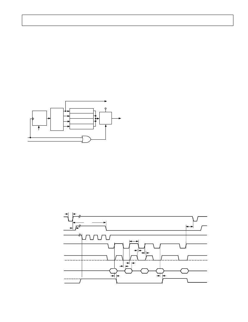
Figure 8. Output Data Registers
When reading the output data registers after a conversion se-
quence, i.e., when BUSY goes low, the register pointer is incre-
mented on the rising edge of the
RD
signal as shown in Figure
8. However, when reading the conversion results between con-
versions in a conversion sequence the pointer will not be incre-
mented until a valid conversion result is in the register to be
addressed. In this case the pointer is incremented when the
conversion has ended and the result has been transferred to the
output data register. This happens when
EOC
goes low, there-
fore
EOC
may be used to enable the register contents onto the
data bus as described in Reading Between Conversions in the
Conversion Sequence. The pointer is reset to point to Register 1
on the rising edge of the
RD
signal when the last conversion
result in the sequence is being read. In the example shown in
Figure 8, this means that the pointer is set to Register 1 when
the contents of Register 3 are read.
Reading After the Conversion Sequence
Figure 9 shows the same conversion sequence as Figure 7. In
this case, however, the results of the four conversions (on V
IN1
to V
IN4
) are read after all conversions have finished, i.e., when
BUSY goes logic low. The FRSTDATA signal goes logic high
at the end of the first conversion just prior to
EOC
going logic
low. As mentioned previously FRSTDATA has an indetermi-
nate state after initial power up, therefore FRSTDATA may
already be logic high. Unlike the case when reading during a
conversion the output data register pointer is incremented on
the rising edge of
RD
because the next conversion result is
available in this case. This means FRSTDATA will go logic low
after the first rising edge on
RD
.
Successive read operations will access the remaining conversion
results in ascending channel order. Each read operation incre-
ments the output data register pointer. The read operation that
accesses the last conversion result causes the output data regis-
ter pointer to be reset so that the next read operation will access
the first conversion result again. This is shown in Figure 8 with
the fifth read after BUSY goes low accessing the result of the
conversion on V
IN1
. Thus the output data registers acts as a
circular buffer in which the conversion results may be continu-
ally accessed. The FRSTDATA signal will go high when the
first conversion result is available.
Data is enabled onto the data bus DB0 to DB13 using
CS
and
RD
. Both
CS
and
RD
have the same functionality as described
in the previous section. There are no restrictions or performance
implications associated with the position of the read operations
after BUSY goes low, however there is a minimum time be-
tween read operations that must be adhered to. Notice also that a
“Quiet Time” is needed before the start of the next conversion
sequence.
t
10
t
8
t
4
t
3
t
6
t
1
QUIET
TIME
DATA
CONVST
BUSY
EOC
FRSTDATA
RD
CS
V
IN2
V
IN3
V
IN1
t
BUSY
t
2
t
10
t
7
V
IN1
V
IN4
Figure 9. Timing Diagram, Reading After the Conversion Sequences
相關PDF資料 |
PDF描述 |
|---|---|
| AD7865AS-2 | Four-Channel, Simultaneous Sampling, Fast, 14-Bit ADC |
| AD7865AS-3 | Four-Channel, Simultaneous Sampling, Fast, 14-Bit ADC |
| AD7865BS-1 | Four-Channel, Simultaneous Sampling, Fast, 14-Bit ADC |
| AD7865BS-2 | Four-Channel, Simultaneous Sampling, Fast, 14-Bit ADC |
| AD7865BS-3 | Four-Channel, Simultaneous Sampling, Fast, 14-Bit ADC |
相關代理商/技術參數 |
參數描述 |
|---|---|
| AD7865AS-1REEL | 制造商:Analog Devices 功能描述:ADC Single SAR 350ksps 14-bit Parallel 44-Pin MQFP T/R 制造商:Rochester Electronics LLC 功能描述:4 CH. SIMULTANEOUS BIPOLAR,14-B ADC I.C. - Tape and Reel |
| AD7865AS2 | 制造商:AD 功能描述:* |
| AD7865AS-2 | 制造商:Analog Devices 功能描述:ADC Single SAR 350ksps 14-bit Parallel 44-Pin MQFP 制造商:Analog Devices 功能描述:IC 14-BIT ADC |
| AD7865AS-2REEL | 制造商:Analog Devices 功能描述:ADC Single SAR 350ksps 14-bit Parallel 44-Pin MQFP T/R 制造商:Analog Devices 功能描述:ADC SGL SAR 350KSPS 14BIT PARALLEL 44MQFP - Tape and Reel |
| AD7865AS-3 | 制造商:Analog Devices 功能描述:ADC Single SAR 350ksps 14-bit Parallel 44-Pin MQFP 制造商:Rochester Electronics LLC 功能描述:4 CH. SIMULTANEOUS BIPOLAR,14-B ADC I.C. - Bulk 制造商:Analog Devices 功能描述:IC 14-BIT ADC |
發布緊急采購,3分鐘左右您將得到回復。