- 您現在的位置:買賣IC網 > PDF目錄373921 > AD7866ARU (ANALOG DEVICES INC) Dual 1 MSPS, 12-Bit, 2-Channel SAR ADC with Serial Interface PDF資料下載
參數資料
| 型號: | AD7866ARU |
| 廠商: | ANALOG DEVICES INC |
| 元件分類: | ADC |
| 英文描述: | Dual 1 MSPS, 12-Bit, 2-Channel SAR ADC with Serial Interface |
| 中文描述: | 4-CH 12-BIT SUCCESSIVE APPROXIMATION ADC, SERIAL ACCESS, PDSO20 |
| 封裝: | MO-153AC, TSSOP-20 |
| 文件頁數: | 10/20頁 |
| 文件大小: | 304K |
| 代理商: | AD7866ARU |
REV. 0
AD7866
–10–
CAPACITIVE
DAC
CONTROL
LOGIC
COMPARATOR
SW2
SW1
A
B
AGND
V
IN
Figure 3. ADC Conversion Phase
ANALOG INPUT
Figure 4 shows an equivalent circuit of the analog input structure
of the AD7866. The two diodes D1 and D2 provide ESD pro-
tection for the analog inputs. Care must be taken to ensure that
the analog input signal never exceeds the supply rails by more
than 300 mV. This will cause these diodes to become forward-
biased and start conducting current into the substrate. 10 mA
is the maximum current these diodes can conduct without causing
irreversible damage to the part. The capacitor C1 in Figure 4
is typically about 10 pF and can primarily be attributed to pin
capacitance. The resistor R1 is a lumped component made up
of the on resistance of a switch. This resistor is typically about
100
. The capacitor C2 is the ADC sampling capacitor and
has a capacitance of 20 pF typically. For ac applications, remov-
ing high-frequency components from the analog input signal is
recommended by use of an RC low-pass filter on the relevant
analog input pin. In applications where harmonic distortion and
signal-to-noise ratio are critical, the analog input should be driven
from a low impedance source. Large source impedances will
significantly affect the ac performance of the ADC. This may
necessitate the use of an input buffer amplifier. The choice of
the op amp will be a function of the particular application.
V
DD
V
IN
C1
D1
D2
R1
CONVERT PHASE
–
SWITCH OPEN
TRACK PHASE
–
SWITCH CLOSED
C2
Figure 4. Equivalent Analog Input Circuit
When no amplifier is used to drive the analog input the source
impedance should be limited to low values. The maximum
source impedance will depend on the amount of total harmonic
distortion (THD) that can be tolerated. The THD will increase
as the source impedance increases and performance will degrade
(see TPC 7).
Analog Input Ranges
The analog input range for the AD7866 can be selected to be 0 V
to V
REF
or 2
×
V
REF
with either straight binary or two’s comple-
ment output coding. The RANGE pin is used to select both the
analog input range and the output coding, as shown in Figures 5
through 8. On the falling edge of
CS
, point A, the logic level of
the RANGE pin is checked to determine the analog input range
of the
next conversion. If this pin is tied to a logic low then the
CIRCUIT INFORMATION
The AD7866 is a fast, micropower, dual 12-bit, single supply,
A/D converter that operates from a 2.7 V to 5.25 V supply.
When operated from either a 5 V supply or a 3 V supply, the
AD7866 is capable of throughput rates of 1 MSPS when provided
with a 20 MHz clock.
The AD7866 contains two on-chip track/hold amplifiers, two
successive-approximation A/D converters, and a serial interface
with two separate data output pins, housed in a 20-lead TSSOP
package, which offers the user considerable space-saving advantages
over alternative solutions. The serial clock input accesses data
from the part but also provides the clock source for each
successive-approximation A/D converter. The analog input range for
the part can be selected to be a 0 V to V
REF
input or a 2
×
V
REF
input
with either straight binary or two’s complement output coding.
The AD7866 has an on-chip 2.5 V reference which can be over-
driven if an external reference is preferred. In addition, each ADC
can be supplied with an individual separate external reference.
The AD7866 also features power-down options to allow power
saving between conversions. The power-down feature is imple-
mented across the standard serial interface as described in the
Modes of Operation section.
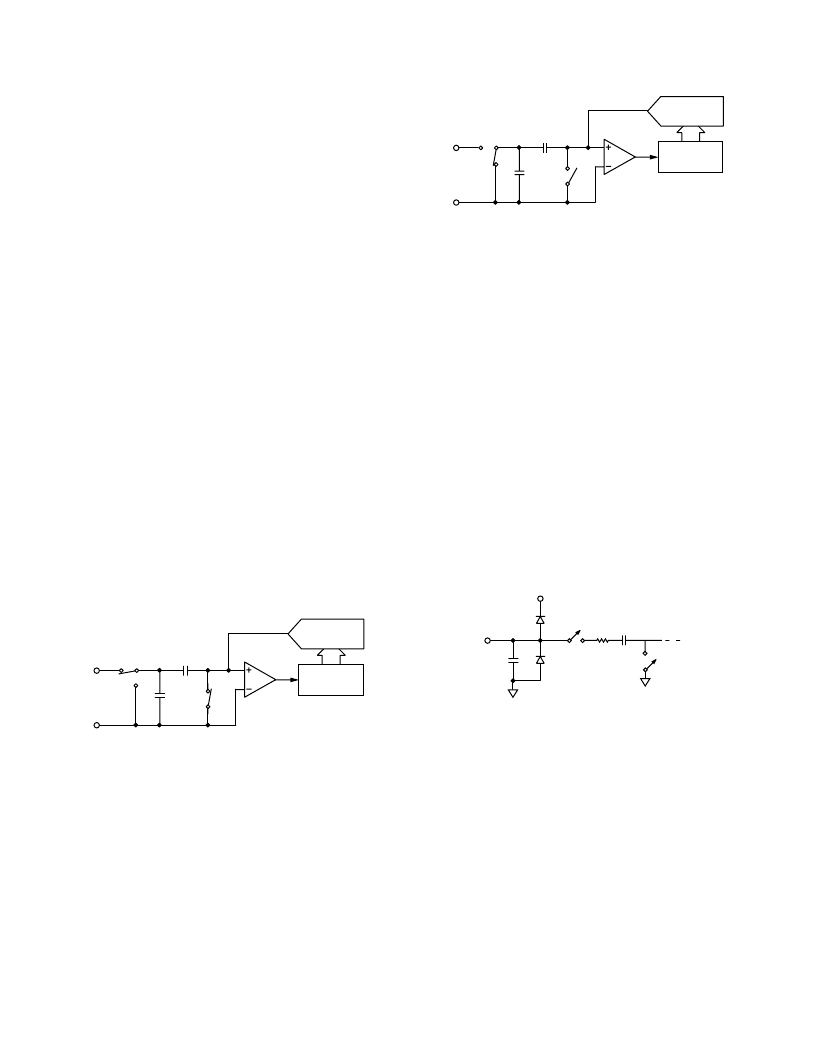
CONVERTER OPERATION
The AD7866 has two successive-approximation analog-to-digital
converters, each based around a capacitive DAC. Figures 2 and 3
show simplified schematics of one of these ADCs. The ADC is
comprised of control logic, a SAR, and a capacitive DAC, all of
which are used to add and subtract fixed amounts of charge from
the sampling capacitor to bring the comparator back into a bal-
anced condition. Figure 2 shows the ADC during its acquisition
phase. SW2 is closed and SW1 is in position A, the comparator is
held in a balanced condition and the sampling capacitor acquires
the signal on V
A1
for example.
CAPACITIVE
DAC
CONTROL
LOGIC
COMPARATOR
SW2
SW1
A
B
AGND
V
IN
Figure 2. ADC Acquisition Phase
When the ADC starts a conversion (see Figure 3), SW2 will
open and SW1 will move to position B causing the comparator
to become unbalanced. The Control Logic and the capacitive
DAC are used to add and subtract fixed amounts of charge
from the sampling capacitor to bring the comparator back
into a balanced condition. When the comparator is rebalanced
the conversion is complete. The Control Logic generates the ADC
output code. Figures 10 and 11 show the ADC transfer functions.
相關PDF資料 |
PDF描述 |
|---|---|
| AD7866BRU | Dual 1 MSPS, 12-Bit, 2-Channel SAR ADC with Serial Interface |
| AD7866 | Dual 1 MSPS, 12-Bit, 2-Channel SAR ADC with Serial Interface |
| AD7868AN | LC2MOS Complete, 12-Bit Analog I/O System |
| AD7868AQ | LC2MOS Complete, 12-Bit Analog I/O System |
| AD7868AR | LC2MOS Complete, 12-Bit Analog I/O System |
相關代理商/技術參數 |
參數描述 |
|---|---|
| AD7866ARU-REEL | 制造商:Analog Devices 功能描述:ADC Dual SAR 1Msps 12-bit Serial 20-Pin TSSOP T/R |
| AD7866ARU-REEL7 | 功能描述:IC ADC 12BIT 2CH DUAL 20TSSOP RoHS:否 類別:集成電路 (IC) >> 數據采集 - 模數轉換器 系列:- 產品培訓模塊:Lead (SnPb) Finish for COTS Obsolescence Mitigation Program 標準包裝:2,500 系列:- 位數:12 采樣率(每秒):3M 數據接口:- 轉換器數目:- 功率耗散(最大):- 電壓電源:- 工作溫度:- 安裝類型:表面貼裝 封裝/外殼:SOT-23-6 供應商設備封裝:SOT-23-6 包裝:帶卷 (TR) 輸入數目和類型:- |
| AD7866ARUZ | 功能描述:IC ADC 12BIT 2CH DUAL 20-TSSOP RoHS:是 類別:集成電路 (IC) >> 數據采集 - 模數轉換器 系列:- 標準包裝:1 系列:microPOWER™ 位數:8 采樣率(每秒):1M 數據接口:串行,SPI? 轉換器數目:1 功率耗散(最大):- 電壓電源:模擬和數字 工作溫度:-40°C ~ 125°C 安裝類型:表面貼裝 封裝/外殼:24-VFQFN 裸露焊盤 供應商設備封裝:24-VQFN 裸露焊盤(4x4) 包裝:Digi-Reel® 輸入數目和類型:8 個單端,單極 產品目錄頁面:892 (CN2011-ZH PDF) 其它名稱:296-25851-6 |
| AD7866ARUZ-REEL | 功能描述:IC ADC 12BIT 2CHAN DUAL 20TSSOP RoHS:是 類別:集成電路 (IC) >> 數據采集 - 模數轉換器 系列:- 標準包裝:1,000 系列:- 位數:16 采樣率(每秒):45k 數據接口:串行 轉換器數目:2 功率耗散(最大):315mW 電壓電源:模擬和數字 工作溫度:0°C ~ 70°C 安裝類型:表面貼裝 封裝/外殼:28-SOIC(0.295",7.50mm 寬) 供應商設備封裝:28-SOIC W 包裝:帶卷 (TR) 輸入數目和類型:2 個單端,單極 |
| AD7866ARUZ-REEL7 | 功能描述:IC ADC 12BIT 2CHAN DUAL 20TSSOP RoHS:是 類別:集成電路 (IC) >> 數據采集 - 模數轉換器 系列:- 標準包裝:1,000 系列:- 位數:16 采樣率(每秒):45k 數據接口:串行 轉換器數目:2 功率耗散(最大):315mW 電壓電源:模擬和數字 工作溫度:0°C ~ 70°C 安裝類型:表面貼裝 封裝/外殼:28-SOIC(0.295",7.50mm 寬) 供應商設備封裝:28-SOIC W 包裝:帶卷 (TR) 輸入數目和類型:2 個單端,單極 |
發布緊急采購,3分鐘左右您將得到回復。