- 您現(xiàn)在的位置:買賣IC網(wǎng) > PDF目錄373921 > AD7866ARU (ANALOG DEVICES INC) Dual 1 MSPS, 12-Bit, 2-Channel SAR ADC with Serial Interface PDF資料下載
參數(shù)資料
| 型號: | AD7866ARU |
| 廠商: | ANALOG DEVICES INC |
| 元件分類: | ADC |
| 英文描述: | Dual 1 MSPS, 12-Bit, 2-Channel SAR ADC with Serial Interface |
| 中文描述: | 4-CH 12-BIT SUCCESSIVE APPROXIMATION ADC, SERIAL ACCESS, PDSO20 |
| 封裝: | MO-153AC, TSSOP-20 |
| 文件頁數(shù): | 4/20頁 |
| 文件大小: | 304K |
| 代理商: | AD7866ARU |
REV. 0
AD7866
TIMING SPECIFICATIONS
1
(V
DD
= 2.7 V to 5.25 V, V
DRIVE
= 2.7 V to 5.25 V, V
REF
= 2.5 V; T
A
= T
MIN
to T
MAX
, unless otherwise noted.)
–4–
1.6V
200 A
I
OL
200 A
I
OH
C
L
50pF
TO
OUTPUT
PIN
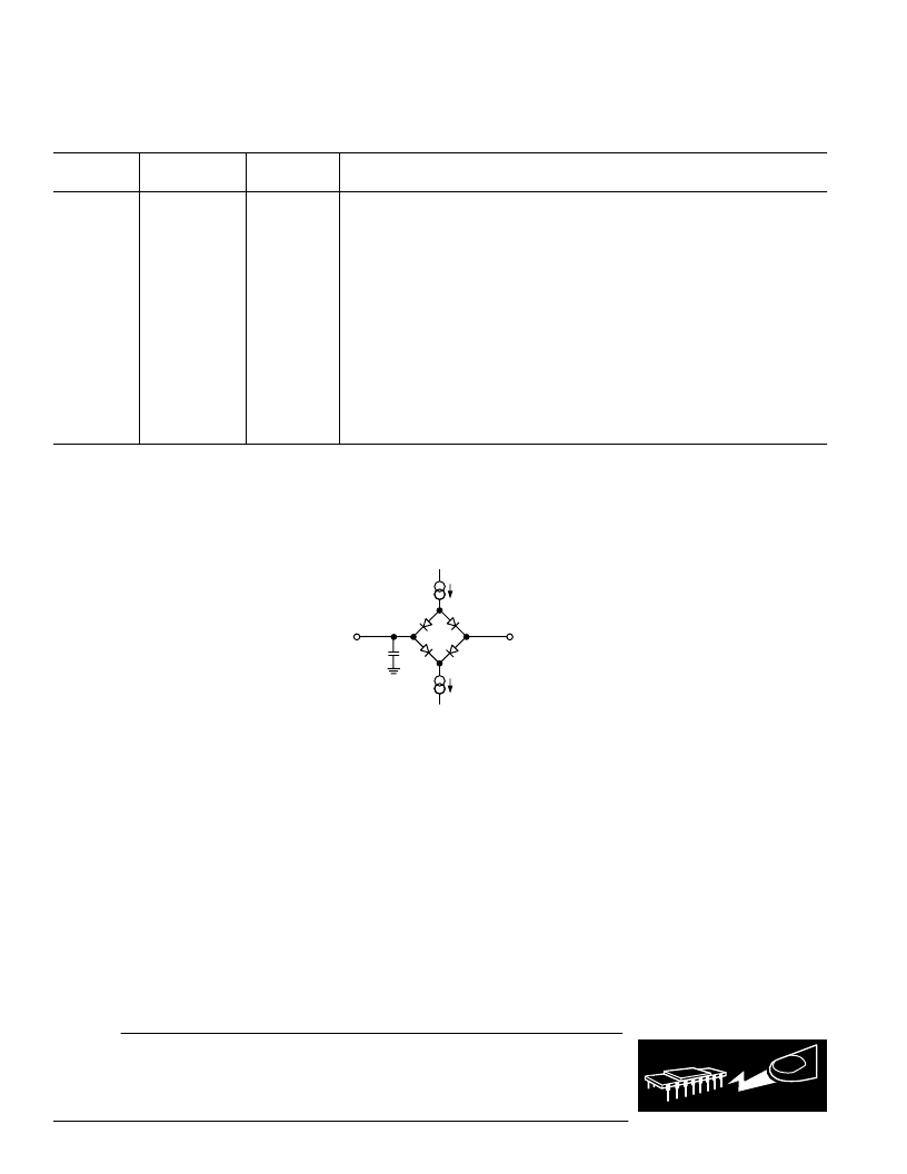
Figure 1. Load Circuit for Digital Output
Timing Specifications
WARNING!
ESD SENSITIVE DEVICE
CAUTION
ESD (electrostatic discharge) sensitive device. Electrostatic charges as high as 4000 V readily
accumulate on the human body and test equipment and can discharge without detection. Although
the AD7866 features proprietary ESD protection circuitry, permanent damage may occur on
devices subjected to high-energy electrostatic discharges. Therefore, proper ESD precautions are
recommended to avoid performance degradation or loss of functionality.
ABSOLUTE MAXIMUM RATINGS
1
(T
A
= 25
o
C unless otherwise noted)
AV
DD
to AGND . . . . . . . . . . . . . . . . . . . . . . . . –0.3 V to +7 V
DV
DD
to DGND . . . . . . . . . . . . . . . . . . . . . . . –0.3 V to +7 V
V
DRIVE
to DGND . . . . . . . . . . . . . . . –0.3 V to DV
DD
+ 0.3 V
V
DRIVE
to AGND . . . . . . . . . . . . . . . . –0.3 V to AV
DD
+ 0.3 V
AV
DD
to DV
DD
. . . . . . . . . . . . . . . . . . . . . . . –0.3 V to +0.3 V
AGND to DGND . . . . . . . . . . . . . . . . . . . . –0.3 V to +0.3 V
Analog Input Voltage to AGND . . . . –0.3 V to AV
DD
+ 0.3 V
Digital Input Voltage to DGND . . . . . . . . . . . –0.3 V to +7 V
V
REF
to AGND . . . . . . . . . . . . . . . . . –0.3 V to AV
DD
+ 0.3 V
Digital Output Voltage to DGND . . –0.3 V to V
DRIVE
+ 0.3 V
Input Current to Any Pin Except Supplies
2
. . . . . . . .
±
10 mA
Operating Temperature Range
Commercial (A, B Versions) . . . . . . . . . . . . . –40
o
C to +85
o
C
Storage Temperature Range . . . . . . . . . . . . –65
o
C to +150
o
C
Junction Temperature . . . . . . . . . . . . . . . . . . . . . . . . . . 150
o
C
TSSOP Package, Power Dissipation . . . . . . . . . . . . . 450 mW
JA
Thermal Impedance . . . . . . . . . . . . 143
°
C/W (TSSOP)
JC
Thermal Impedance . . . . . . . . . . . . . 45
°
C/W (TSSOP)
Lead Temperature, Soldering
Vapor Phase (60 secs) . . . . . . . . . . . . . . . . . . . . . . . 215
°
C
Infrared (15 secs) . . . . . . . . . . . . . . . . . . . . . . . . . . 220
°
C
ESD . . . . . . . . . . . . . . . . . . . . . . . . . . . . . . . . . . . . . . . 1.5 kV
NOTES
1
Stresses above those listed under Absolute Maximum Ratings may cause permanent
damage to the device. This is a stress rating only; functional operation of the device
at these or any other conditions above those listed in the operational sections of this
specification is not implied. Exposure to absolute maximum rating conditions for
extended periods may affect device reliability.
2
Transient currents of up to 100 mA will not cause SCR latch up.
Limit at
T
MIN
, T
MAX
10
20
16
×
t
SCLK
800
50
10
25
40
Parameter
f
SCLK 2
Unit
Description
kHz min
MHz max
ns max
ns max
ns max
ns min
ns max
ns max
t
CONVERT
t
SCLK
= 1/f
SCLK
f
SCLK
= 20 MHz
Minimum Time Between End of Serial Read and Next Falling Edge of
CS
CS
to SCLK Setup Time
Delay from
CS
Until D
OUT
A and D
OUT
B Three-State Disabled
Data Access Time After SCLK Falling Edge. V
DRIVE
3 V, C
L
= 50 pF;
V
DRIVE
< 3 V, C
L
= 25 pF
SCLK Low Pulsewidth
SCLK High Pulsewidth
SCLK to Data Valid Hold Time
CS
Rising Edge to D
OUT
A, D
OUT
B, High Impedance
SCLK Falling Edge to D
OUT
A, D
OUT
B, High Impedance
SCLK Falling Edge to D
OUT
A, D
OUT
B, High Impedance
t
QUIET
t
2
t
33
t
43
t
5
t
6
t
7
t
84
t
94
0.4 t
SCLK
0.4 t
SCLK
10
25
10
50
ns min
ns min
ns min
ns max
ns min
ns max
NOTES
1
Sample tested at 25
°
C to ensure compliance. All input signals are specified with tr = tf = 5 ns (10% to 90% of V
DRIVE
) and timed from a voltage level of 1.6 V.
2
Mark/Space ratio for the CLK input is 40/60 to 60/40.
3
Measured with the load circuit of Figure 1 and defined as the time required for the output to cross 0.8 V or 2.0 V.
4
t
t
are derived from the measured time taken by the data outputs to change 0.5 V when loaded with the circuit of Figure 1. The measured number is then extrapolated
back to remove the effects of charging or discharging the 50 pF capacitor. This means that the times t
8
and t
9
quoted in the timing characteristics are the true bus
relinquish times of the part and are independent of the bus loading.
Specifications subject to change without notice.
相關PDF資料 |
PDF描述 |
|---|---|
| AD7866BRU | Dual 1 MSPS, 12-Bit, 2-Channel SAR ADC with Serial Interface |
| AD7866 | Dual 1 MSPS, 12-Bit, 2-Channel SAR ADC with Serial Interface |
| AD7868AN | LC2MOS Complete, 12-Bit Analog I/O System |
| AD7868AQ | LC2MOS Complete, 12-Bit Analog I/O System |
| AD7868AR | LC2MOS Complete, 12-Bit Analog I/O System |
相關代理商/技術參數(shù) |
參數(shù)描述 |
|---|---|
| AD7866ARU-REEL | 制造商:Analog Devices 功能描述:ADC Dual SAR 1Msps 12-bit Serial 20-Pin TSSOP T/R |
| AD7866ARU-REEL7 | 功能描述:IC ADC 12BIT 2CH DUAL 20TSSOP RoHS:否 類別:集成電路 (IC) >> 數(shù)據(jù)采集 - 模數(shù)轉(zhuǎn)換器 系列:- 產(chǎn)品培訓模塊:Lead (SnPb) Finish for COTS Obsolescence Mitigation Program 標準包裝:2,500 系列:- 位數(shù):12 采樣率(每秒):3M 數(shù)據(jù)接口:- 轉(zhuǎn)換器數(shù)目:- 功率耗散(最大):- 電壓電源:- 工作溫度:- 安裝類型:表面貼裝 封裝/外殼:SOT-23-6 供應商設備封裝:SOT-23-6 包裝:帶卷 (TR) 輸入數(shù)目和類型:- |
| AD7866ARUZ | 功能描述:IC ADC 12BIT 2CH DUAL 20-TSSOP RoHS:是 類別:集成電路 (IC) >> 數(shù)據(jù)采集 - 模數(shù)轉(zhuǎn)換器 系列:- 標準包裝:1 系列:microPOWER™ 位數(shù):8 采樣率(每秒):1M 數(shù)據(jù)接口:串行,SPI? 轉(zhuǎn)換器數(shù)目:1 功率耗散(最大):- 電壓電源:模擬和數(shù)字 工作溫度:-40°C ~ 125°C 安裝類型:表面貼裝 封裝/外殼:24-VFQFN 裸露焊盤 供應商設備封裝:24-VQFN 裸露焊盤(4x4) 包裝:Digi-Reel® 輸入數(shù)目和類型:8 個單端,單極 產(chǎn)品目錄頁面:892 (CN2011-ZH PDF) 其它名稱:296-25851-6 |
| AD7866ARUZ-REEL | 功能描述:IC ADC 12BIT 2CHAN DUAL 20TSSOP RoHS:是 類別:集成電路 (IC) >> 數(shù)據(jù)采集 - 模數(shù)轉(zhuǎn)換器 系列:- 標準包裝:1,000 系列:- 位數(shù):16 采樣率(每秒):45k 數(shù)據(jù)接口:串行 轉(zhuǎn)換器數(shù)目:2 功率耗散(最大):315mW 電壓電源:模擬和數(shù)字 工作溫度:0°C ~ 70°C 安裝類型:表面貼裝 封裝/外殼:28-SOIC(0.295",7.50mm 寬) 供應商設備封裝:28-SOIC W 包裝:帶卷 (TR) 輸入數(shù)目和類型:2 個單端,單極 |
| AD7866ARUZ-REEL7 | 功能描述:IC ADC 12BIT 2CHAN DUAL 20TSSOP RoHS:是 類別:集成電路 (IC) >> 數(shù)據(jù)采集 - 模數(shù)轉(zhuǎn)換器 系列:- 標準包裝:1,000 系列:- 位數(shù):16 采樣率(每秒):45k 數(shù)據(jù)接口:串行 轉(zhuǎn)換器數(shù)目:2 功率耗散(最大):315mW 電壓電源:模擬和數(shù)字 工作溫度:0°C ~ 70°C 安裝類型:表面貼裝 封裝/外殼:28-SOIC(0.295",7.50mm 寬) 供應商設備封裝:28-SOIC W 包裝:帶卷 (TR) 輸入數(shù)目和類型:2 個單端,單極 |
發(fā)布緊急采購,3分鐘左右您將得到回復。