- 您現在的位置:買賣IC網 > PDF目錄373921 > AD7868BQ (ANALOG DEVICES INC) LC2MOS Complete, 12-Bit Analog I/O System PDF資料下載
參數資料
| 型號: | AD7868BQ |
| 廠商: | ANALOG DEVICES INC |
| 元件分類: | 模擬信號調理 |
| 英文描述: | LC2MOS Complete, 12-Bit Analog I/O System |
| 中文描述: | SPECIALTY ANALOG CIRCUIT, CDIP24 |
| 封裝: | CERDIP-24 |
| 文件頁數: | 6/16頁 |
| 文件大小: | 337K |
| 代理商: | AD7868BQ |
AD7868
–6–
REV. B
CONVE RT E R DE T AILS
T he AD7868 is a complete 12-bit I/O port, the only external
components required for normal operation are pull-up resistors
for the ADC data outputs and power supply decoupling capaci-
tors. It is comprised of a 12-bit successive approximation ADC
with a track/hold amplifier, a 12-bit DAC with a buffered output
and two 3 V buried Zener references, a clock oscillator and con-
trol logic.
ADC CLOCK
T he AD7868 has an internal clock oscillator which can be used
for the ADC conversion procedure. T he oscillator is enabled by
tying the CLK input to V
SS
. T he oscillator in laser trimmed at
the factory to give a conversion time of between 8.5 and 10
μ
s.
T he mark/space ratio can vary from 40/60 to 60/40. Alterna-
tively, an external T T L compatible clock may be applied to this
input. T he allowable mark/space ratio of an external clock is
40/60 to 60/40. RCLK is a clock output, used for the serial in-
terface. T his output is derived directly from the ADC clock
source and can be switched off at the end of conversion with the
CONT ROL input.
ADC CONVE RSION T IMING
T he conversion time for both external clock and continuous in-
ternal clock can vary from 19 to 20 rising clock edges depending
on the conversion start to ADC clock synchronization. If a con-
version is initiated within 30 ns prior to a rising edge of the ADC
clock, the conversion time will consist of 20 rising clock edges,
i.e., 9.5
μ
s conversion time. For noncontinuous internal clock,
the conversion time is always 19 rising clock edges.
ADC T RACK -AND-HOLD AMPLIFIE R
T he track-and-hold amplifier on the analog input of the AD7868
allows the ADC to accurately convert an input sine wave of 6 V
peak–peak amplitude to 12-bit accuracy. T he input impedance is
typically 9 k
, an equivalent circuit is shown in Figure 1. T he
input bandwidth of the track/hold amplifier is much greater than
the Nyquist rate of the ADC, even when the ADC is operated at
its maximum throughput rate. T he 0.1 dB cutoff frequency oc-
curs typically at 500 kHz. T he track/hold amplifier acquires an
input signal to 12-bit accuracy in less than 2
μ
s.
AD7868*
4.5k
*ADDITIONAL PINS OMITTED FOR CLARITY
V
IN
TO INTERNAL
COMPARATOR
TRACK/HOLD
AMPLIFIER
TO INTERNAL
3V REFERENCE
4.5k
Figure 1. ADC Analog Input
T he overall throughput rate is equal to the conversion time plus
the track/hold amplifier acquisition time. For a 2.0 MHz input
clock the throughput time is 12
μ
s max.
T he operation of the track/hold amplifier is essentially transpar-
ent to the user. T he track/hold amplifier goes from its track
mode to its hold mode at the start of conversion on the rising
edge of
CONVST
.
INT E RNAL RE FE RE NCE S
T he AD7868 has two on-chip temperature compensated buried
Zener references which are factory trimmed to 3 V
±
10 mV.
One reference provides the appropriate biasing for the ADC,
while the other is available as a reference of the DAC. Both ref-
erence outputs are available (labeled RO DAC and RO ADC)
and are capable of providing up to 500
μ
A to an external load.
T he DAC input reference (RI DAC) can be stored externally or
connected to any of the two on-chip references. Applications
requiring good full-scale error matching between the DAC and
the ADC should use the ADC reference as shown in Figure 4.
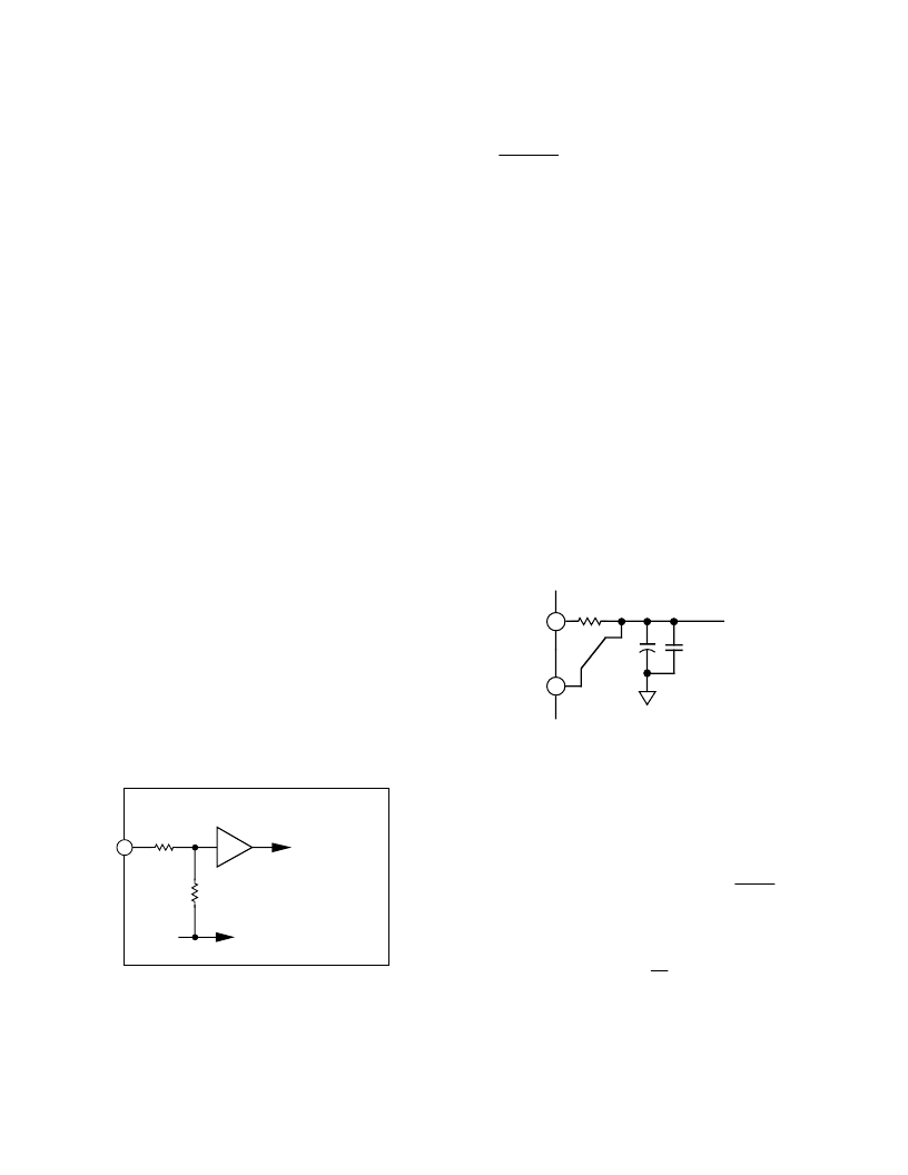
T he maximum recommended capacitance on either of the refer-
ence output pins for normal operation is 50 pF. If either of the
reference outputs is required to drive a capacitive load greater
than 50 pF, then a 200
resistor must be placed in series with
the capacitive load. T he addition of decoupling capacitors,
10
μ
F in parallel with 0.1
μ
F, as shown in Figure 2, improves
noise performance. T he improvement in noise performance can
be seen from the graph in Figure 3. Note, this applies for the
DAC output only; reference decoupling components do not af-
fect ADC performance. So, a typical application will have just
the DAC reference source decoupled with the other one open
circuited.
RI DAC
200
10
μ
F
0.1
μ
F
RO DAC
or
RO ADC*
EXT LOAD
GREATER THAN 50pF
*RO DAC/RO ADC CAN BE LEFT
OPEN CIRCUIT IF NOT USED
Figure 2. Reference Decoupling Circuitry
DAC OUT PUT AMPLIFIE R
T he output from the voltage-mode DAC is buffered by a nonin-
verting amplifier. T he buffer amplifier is capable of developing
±
3 V across 2 k
and 100 pF load to ground and can produce
6 V peak-to-peak sine wave signals to a frequency of 20 kHz.
T he output is updated on the falling edge of the
LDAC
input.
T he output voltage settling time, to within 1/2 LSB of its final
value, is typically less than 2
μ
s.
T he small signal (200 mV p-p) bandwidth of the output buffer
amplifier is typically 1 MHz. T he output noise from the ampli-
fier is low with a figure of 30 nV/
√
Hz
at a frequency of 1 kHz.
T he broadband noise from the amplifier exhibits a typical peak-
to-peak figure of 150
μ
V for a 1 MHz output bandwidth. Fig-
ure 3 shows a typical plot of noise spectral density versus fre-
quency for the output buffer amplifier and for either of the
on-chip references.
相關PDF資料 |
PDF描述 |
|---|---|
| AD7868BR | LC2MOS Complete, 12-Bit Analog I/O System |
| AD7869AQ | LC2MOS Complete, 14-Bit Analog I/O System |
| AD7869JN | LC2MOS Complete, 14-Bit Analog I/O System |
| AD7869JR | LC2MOS Complete, 14-Bit Analog I/O System |
| AD7870A | Complete, 12-Bit, 100 kHz , Sampling ADC(完備的,頻率為100kHz,12位A/D轉換器) |
相關代理商/技術參數 |
參數描述 |
|---|---|
| AD7868BR | 制造商:Analog Devices 功能描述:Data Acquisition System Single ADC Single DAC 12-Bit 28-Pin SOIC W 制造商:Rochester Electronics LLC 功能描述:ANALOG I/O PORT IC - Bulk |
| AD7868BR-REEL | 功能描述:IC I/O PORT 12BIT ANLG 28-SOIC RoHS:否 類別:集成電路 (IC) >> 接口 - 專用 系列:- 標準包裝:3,000 系列:- 應用:PDA,便攜式音頻/視頻,智能電話 接口:I²C,2 線串口 電源電壓:1.65 V ~ 3.6 V 封裝/外殼:24-WQFN 裸露焊盤 供應商設備封裝:24-QFN 裸露焊盤(4x4) 包裝:帶卷 (TR) 安裝類型:表面貼裝 產品目錄頁面:1015 (CN2011-ZH PDF) 其它名稱:296-25223-2 |
| AD7868BRZ | 功能描述:IC I/O PORT 12BIT ANLG 28SOIC RoHS:是 類別:集成電路 (IC) >> 接口 - 專用 系列:- 標準包裝:3,000 系列:- 應用:PDA,便攜式音頻/視頻,智能電話 接口:I²C,2 線串口 電源電壓:1.65 V ~ 3.6 V 封裝/外殼:24-WQFN 裸露焊盤 供應商設備封裝:24-QFN 裸露焊盤(4x4) 包裝:帶卷 (TR) 安裝類型:表面貼裝 產品目錄頁面:1015 (CN2011-ZH PDF) 其它名稱:296-25223-2 |
| AD7868BRZ-REEL | 功能描述:IC I/O PORT 12BIT ANLG 28SOIC RoHS:是 類別:集成電路 (IC) >> 接口 - 專用 系列:- 標準包裝:3,000 系列:- 應用:PDA,便攜式音頻/視頻,智能電話 接口:I²C,2 線串口 電源電壓:1.65 V ~ 3.6 V 封裝/外殼:24-WQFN 裸露焊盤 供應商設備封裝:24-QFN 裸露焊盤(4x4) 包裝:帶卷 (TR) 安裝類型:表面貼裝 產品目錄頁面:1015 (CN2011-ZH PDF) 其它名稱:296-25223-2 |
| AD7868TQ/883B | 制造商:未知廠家 制造商全稱:未知廠家 功能描述:CODEC, Single |
發布緊急采購,3分鐘左右您將得到回復。