- 您現在的位置:買賣IC網 > PDF目錄373921 > AD7868BQ (ANALOG DEVICES INC) LC2MOS Complete, 12-Bit Analog I/O System PDF資料下載
參數資料
| 型號: | AD7868BQ |
| 廠商: | ANALOG DEVICES INC |
| 元件分類: | 模擬信號調理 |
| 英文描述: | LC2MOS Complete, 12-Bit Analog I/O System |
| 中文描述: | SPECIALTY ANALOG CIRCUIT, CDIP24 |
| 封裝: | CERDIP-24 |
| 文件頁數: | 8/16頁 |
| 文件大小: | 337K |
| 代理商: | AD7868BQ |
AD7868
–8–
REV. B
T IMING AND CONT ROL
Communication with the AD7868 is managed by 6 dedicated
pins. T hese consist of separate serial clocks, word framing or
strobe pulses and data signals for both receiving and transmit-
ting data. Conversion starts and DAC updating are controlled
by two digital inputs;
CONVST
and
LDAC
. T hese inputs can
be asserted independently of the microprocessor by an external
timer when precise sampling intervals are required. Alterna-
tively, the
LDAC
and
CONVST
can be driven from a decoded
address bus allowing the microprocessor control over conversion
start and DAC updating as well as data communication to the
AD7868.
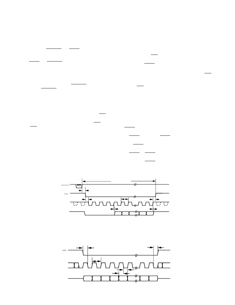
ADC T iming
Conversion control is provided by the
CONVST
input. A low to
high transition on
CONVST
input starts conversion and drives
the track/hold amplifier into its hold mode. Serial data then be-
comes available while conversion is in progress. T he correspond-
ing timing diagram is shown in Figure 7. T he word length is 16
bits; 4 leading zeros, followed by the 12-bit conversion result
starting with the MSB. T he data is synchronized to the serial
clock output (RCLK ) and is framed by the serial strobe (
RFS
).
Data is clocked out on a low to high transition of the serial clock
and is valid on the falling edge of this clock while the
RFS
out-
put is low.
RFS
goes low at the start of conversion and the first
serial data bit (which is the first leading zero) is valid on the first
falling edge of RCLK . All the ADC serial lines are open-drain
outputs and require external pull-up resistors.
T he serial clock out is derived from the ADC master clock
source which may be internal or external. Normally, RCLK is
required during the serial transmission only. In these cases it can
be shut down (i.e., placed into high impedance) at the end of
conversion to allow multiple ADCs to share a common serial
bus. However, some serial systems (e.g., T MS32020) require a
serial clock which runs continuously. Both options are available
on the AD7868 ADC. With the CONT ROL input at 0 V, RCLK
is noncontinuous and when it is at –5 V, RCLK is continuous.
DAC T iming
T he AD7868 DAC contains two latches, an input latch and a
DAC latch. Data must be loaded to the input latch under the
control of the T CLK ,
TFS
and DT serial logic inputs. Data is
then transferred from the input latch to the DAC latch under
the control of the
LDAC
signal. Only the data in the DAC latch
determines the analog output of the AD7868.
Data is loaded to the input latch under control of T CLK ,
TFS
and DT . T he AD7868 DAC expects a 16-bit stream of serial
data on its DT input. Data must be valid on the falling edge of
T CLK . T he
TFS
input provides the frame synchronization sig-
nal which tells the AD7868 DAC that valid serial data will be
available for the next 16 falling edges of T CLK . Figure 8 shows
the timing diagram for the serial data format.
Although 16 bits of data are clocked into the input latch, only
12 bits are transferred into the DAC latch. T herefore, 4 bits in
the stream are don’t cares since their value does not affect the
DAC latch data. T he bit positions are 4 don’t cares followed by
the 12-bit DAC data starting with the MSB.
T he
LDAC
signal controls the transfer of data to the DAC
latch. Normally, data is loaded to the DAC latch on the falling
edge of
LDAC
. However, if
LDAC
is held low, then serial data
is loaded to the DAC latch on the sixteenth falling edge of
T CLK . If
LDAC
goes low during the loading of serial data to
the input latch, no DAC latch update takes place on the falling
edge of
LDAC
. If
LDAC
stays low until the serial transfer is
completed, then the update takes place on the sixteenth falling
edge of T CLK . If
LDAC
returns high before the serial data
transfer is completed, no DAC latch update takes place.
NOTES
1
EXTERNAL 4.7k
PULL-UP RESISTOR
2
EXTERNAL 2k
PULL-UP RESISTOR
3
CONTINUOUS RCLK (DASHED LINE) WHEN THE CONTROL INPUT = –5V AND
NONCONTINUOUS WHEN THE CONTROL INPUT = 0V
t
13
t
3
CONVST
RFS
1
RCLK
2, 3
DR
1
DB11
DB10
DB9
DB1
DB0
CONVERSION TIME
t
1
t
5
t
2
t
4
t
6
Figure 7. ADC Control Timing Diagram
DB11
DB10
DB1
DB0
t
7
t
8
t
9
t
10
t
11
TFS
TCLK
DT
DON'T
DON'T
DON'T
DON'T
Figure 8. DAC Control Timing Diagram
相關PDF資料 |
PDF描述 |
|---|---|
| AD7868BR | LC2MOS Complete, 12-Bit Analog I/O System |
| AD7869AQ | LC2MOS Complete, 14-Bit Analog I/O System |
| AD7869JN | LC2MOS Complete, 14-Bit Analog I/O System |
| AD7869JR | LC2MOS Complete, 14-Bit Analog I/O System |
| AD7870A | Complete, 12-Bit, 100 kHz , Sampling ADC(完備的,頻率為100kHz,12位A/D轉換器) |
相關代理商/技術參數 |
參數描述 |
|---|---|
| AD7868BR | 制造商:Analog Devices 功能描述:Data Acquisition System Single ADC Single DAC 12-Bit 28-Pin SOIC W 制造商:Rochester Electronics LLC 功能描述:ANALOG I/O PORT IC - Bulk |
| AD7868BR-REEL | 功能描述:IC I/O PORT 12BIT ANLG 28-SOIC RoHS:否 類別:集成電路 (IC) >> 接口 - 專用 系列:- 標準包裝:3,000 系列:- 應用:PDA,便攜式音頻/視頻,智能電話 接口:I²C,2 線串口 電源電壓:1.65 V ~ 3.6 V 封裝/外殼:24-WQFN 裸露焊盤 供應商設備封裝:24-QFN 裸露焊盤(4x4) 包裝:帶卷 (TR) 安裝類型:表面貼裝 產品目錄頁面:1015 (CN2011-ZH PDF) 其它名稱:296-25223-2 |
| AD7868BRZ | 功能描述:IC I/O PORT 12BIT ANLG 28SOIC RoHS:是 類別:集成電路 (IC) >> 接口 - 專用 系列:- 標準包裝:3,000 系列:- 應用:PDA,便攜式音頻/視頻,智能電話 接口:I²C,2 線串口 電源電壓:1.65 V ~ 3.6 V 封裝/外殼:24-WQFN 裸露焊盤 供應商設備封裝:24-QFN 裸露焊盤(4x4) 包裝:帶卷 (TR) 安裝類型:表面貼裝 產品目錄頁面:1015 (CN2011-ZH PDF) 其它名稱:296-25223-2 |
| AD7868BRZ-REEL | 功能描述:IC I/O PORT 12BIT ANLG 28SOIC RoHS:是 類別:集成電路 (IC) >> 接口 - 專用 系列:- 標準包裝:3,000 系列:- 應用:PDA,便攜式音頻/視頻,智能電話 接口:I²C,2 線串口 電源電壓:1.65 V ~ 3.6 V 封裝/外殼:24-WQFN 裸露焊盤 供應商設備封裝:24-QFN 裸露焊盤(4x4) 包裝:帶卷 (TR) 安裝類型:表面貼裝 產品目錄頁面:1015 (CN2011-ZH PDF) 其它名稱:296-25223-2 |
| AD7868TQ/883B | 制造商:未知廠家 制造商全稱:未知廠家 功能描述:CODEC, Single |
發布緊急采購,3分鐘左右您將得到回復。