- 您現在的位置:買賣IC網 > PDF目錄373923 > AD7884BP (ANALOG DEVICES INC) LC2MOS 16-Bit, High Speed Sampling ADCs PDF資料下載
參數資料
| 型號: | AD7884BP |
| 廠商: | ANALOG DEVICES INC |
| 元件分類: | ADC |
| 英文描述: | LC2MOS 16-Bit, High Speed Sampling ADCs |
| 中文描述: | 2-CH 16-BIT FLASH METHOD ADC, PARALLEL ACCESS, PQCC44 |
| 封裝: | PLASTIC, LCC-44 |
| 文件頁數: | 7/16頁 |
| 文件大小: | 319K |
| 代理商: | AD7884BP |
AD7884/AD7885
REV. C
–7–
T E RMINOLOGY
Integral Nonlinearity
T his is the maximum deviation from a straight line passing
through the endpoints of the ADC transfer function.
Differential Nonlinearity
T his is the difference between the measured and the ideal 1 LSB
change between any two adjacent codes in the ADC.
Bipolar Zero E rror
T his is the deviation of the midscale transition (all 0s to all 1s)
from the ideal (AGND).
Positive Gain E rror
T his is the deviation of the last code transition (01 . . . 110 to
01 . . . 111) from the ideal (+V
REF+
S – 1 LSB), after Bipolar
Zero Error has been adjusted out.
Negative Gain E rror
T his is the deviation of the first code transition (10 . . . 000 to
10 . . . 001) from the ideal (–V
REF+
S + 1 LSB), after Bipolar
Zero Error has been adjusted out.
Signal to (Noise + Distortion) Ratio
T his is the measured ratio of signal to (noise + distortion) at the
output of the A/D converter. T he signal is the rms amplitude of
the fundamental. Noise is the rms sum of all nonfundamental
signals up to half the sampling frequency (f
S
/2), excluding dc.
T he ratio is dependent upon the number of quantization levels
in the digitization process; the more levels, the smaller the quan-
tization noise. T he theoretical signal to (noise + distortion) ratio
for an ideal N-bit converter with a sine wave input is given by:
S
ignal to (Noise + Distortion) = (
6.02
N +
1.76
) dB
T hus for an ideal 16-bit converter, this is 98 dB.
T otal Harmonic Distortion
T otal harmonic distortion (T HD) is the ratio of the rms sum of
harmonics to the fundamental. For the AD7884/AD7885, it is
defined as:
THD
(
dB
)
=
20log
V
2
2
+
V
3
2
+
V
4
V
1
2
+
V
5
2
+
V
6
2
where
V
1
is the rms amplitude of the fundamental and
V
2
,
V
3
,
V
4
,
V
5
and
V
6
are the rms amplitudes of the second through the
sixth harmonics.
Peak Harmonic or Spurious Noise
Peak harmonic or spurious noise is defined as the ratio of the
rms value of the next largest component in the ADC output
spectrum (up to f
S
/2 and excluding dc) to the rms value of the
fundamental. Normally, the value of this specification is deter-
mined by the largest harmonic in the spectrum, but for parts
where the harmonics are buried in the noise floor, it will be a
noise peak.
Intermodulation Distortion
With inputs consisting of sine waves at two frequencies, fa and
fb, any active device with nonlinearities will create distortion
products at sum and difference frequencies of mfa
±
nfb where
m, n = 0, 1, 2, 3, etc. Intermodulation terms are those for which
neither m or n are equal to zero. For example, the second order
terms include (fa + fb) and (fa – fb), while the third order terms
include (2fa + fb), (2fa – fb), (fa + 2fb) and (fa – 2fb).
T he AD7884/AD7885 is tested using the CCIFF standard
where two input frequencies near the top end of the input band-
width are used. In this case, the second and third order terms
are of different significance. T he second order terms are usually
distanced in frequency from the original sine waves while the
third order terms are usually at a frequency close to the input
frequencies. As a result, the second and third order terms are
specified separately. T he calculation of the intermodulation dis-
tortion is as per the T HD specification where it is the ratio of
the rms sum of the individual distortion products to the rms am-
plitude of the fundamental expressed in dBs.
Power Supply Rejection Ratio
T his is the ratio, in dBs, of the change in positive gain error to
the change in V
DD
or V
SS
. It is a dc measurement.
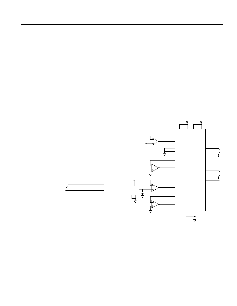
OPE RAT IONAL DIAGRAM
An operational diagram for the AD7884/AD7885 is shown in
Figure 6. It is set up for an analog input range of
±
5 V. If a
±
3 V input range is required, A1 should drive
±
3 V
IN
S and
±
3 V
IN
F with
±
5 V
IN
S,
±
5 V
IN
F being tied to system AGND.
±3V
IN
F
±5V
IN
F
–5V
+5V
AD817
AD711
AD817
AGNDS
AGNDF
AD7884
AD7885
A1
A3
A4
AD845, AD817 OR
EQUIVALENT
NOTE: POWER SUPPLY DECOUPLING NOT SHOWN
A2
GND
DGND
V
DD
= +5V
DATA
OUTPUTS
CONTROL
INPUTS
V
INV
V
REF+
S
V
REF+
F
V
REF–
±3V
IN
S
±5V
IN
S
AV
SS
V
DD
AV
DD
V
SS
V
IN
AD845, AD817 OR
EQUIVALENT
AD780
2
6
8
4
10μF
Figure 6. AD7884/AD7885 Operational Diagram
T he chosen input buffer amplifier (A1) should have low noise
and distortion and fast settling time for high bandwidth applica-
tions. Both the AD711 and the AD845 are suitable amplifiers.
A2 is the force, sense amplifier for AGND. T he AGNDS pin
should be at zero potential. T herefore, the amplifier must have a
low input offset voltage and good noise performance. It must
also have the ability to deal with fast current transients on the
AGNDS pin. T he AD817 has the required performance and is
the recommended amplifier.
If AGNDS and AGNDF are simply tied together to Star
Ground instead of buffering, the SNR and T HD are not signifi-
cantly degraded. However, dc specifications like INL, Bipolar
Zero and Gain Error will be degraded.
相關PDF資料 |
PDF描述 |
|---|---|
| AD7885 | LC2MOS 16-Bit, High Speed Sampling ADCs |
| AD7885AAP | LC2MOS 16-Bit, High Speed Sampling ADCs |
| AD7885ABP | LC2MOS 16-Bit, High Speed Sampling ADCs |
| AD7885AN | LC2MOS 16-Bit, High Speed Sampling ADCs |
| AD7885BN | LC2MOS 16-Bit, High Speed Sampling ADCs |
相關代理商/技術參數 |
參數描述 |
|---|---|
| AD7884BP-REEL | 制造商:Analog Devices 功能描述:ADC Single 2-Step Flash 166ksps 16-bit Parallel 44-Pin PLCC T/R 制造商:Analog Devices 功能描述:16-BIT PARAL.SAMPL ADC - Tape and Reel 制造商:Rochester Electronics LLC 功能描述:16-BIT PARAL.SAMPL ADC - Tape and Reel |
| AD7884BPZ | 功能描述:IC ADC 16BIT SAMPLING HS 44-PLCC RoHS:是 類別:集成電路 (IC) >> 數據采集 - 模數轉換器 系列:- 其它有關文件:TSA1204 View All Specifications 標準包裝:1 系列:- 位數:12 采樣率(每秒):20M 數據接口:并聯 轉換器數目:2 功率耗散(最大):155mW 電壓電源:模擬和數字 工作溫度:-40°C ~ 85°C 安裝類型:表面貼裝 封裝/外殼:48-TQFP 供應商設備封裝:48-TQFP(7x7) 包裝:Digi-Reel® 輸入數目和類型:4 個單端,單極;2 個差分,單極 產品目錄頁面:1156 (CN2011-ZH PDF) 其它名稱:497-5435-6 |
| AD7884BPZ-REEL | 功能描述:IC ADC 16BIT SAMPLING HS 44-PLCC RoHS:是 類別:集成電路 (IC) >> 數據采集 - 模數轉換器 系列:- 產品培訓模塊:Lead (SnPb) Finish for COTS Obsolescence Mitigation Program 標準包裝:250 系列:- 位數:12 采樣率(每秒):1.8M 數據接口:并聯 轉換器數目:1 功率耗散(最大):1.82W 電壓電源:模擬和數字 工作溫度:-40°C ~ 85°C 安裝類型:表面貼裝 封裝/外殼:48-LQFP 供應商設備封裝:48-LQFP(7x7) 包裝:管件 輸入數目和類型:2 個單端,單極 |
| AD7884BQ | 功能描述:IC ADC 16BIT SAMPLING HS 40-CDIP RoHS:否 類別:集成電路 (IC) >> 數據采集 - 模數轉換器 系列:- 產品培訓模塊:Lead (SnPb) Finish for COTS Obsolescence Mitigation Program 標準包裝:2,500 系列:- 位數:12 采樣率(每秒):3M 數據接口:- 轉換器數目:- 功率耗散(最大):- 電壓電源:- 工作溫度:- 安裝類型:表面貼裝 封裝/外殼:SOT-23-6 供應商設備封裝:SOT-23-6 包裝:帶卷 (TR) 輸入數目和類型:- |
| AD7885AAP | 制造商:Analog Devices 功能描述:16-Bit, High Speed Sampling ADCs |
發布緊急采購,3分鐘左右您將得到回復。