- 您現(xiàn)在的位置:買賣IC網(wǎng) > PDF目錄373925 > AD7896SQ (ANALOG DEVICES INC) 2.7 V to 5.5 V, 12-Bit, 8 us ADC in 8-Pin SO/DIP PDF資料下載
參數(shù)資料
| 型號(hào): | AD7896SQ |
| 廠商: | ANALOG DEVICES INC |
| 元件分類: | ADC |
| 英文描述: | 2.7 V to 5.5 V, 12-Bit, 8 us ADC in 8-Pin SO/DIP |
| 中文描述: | 1-CH 12-BIT SUCCESSIVE APPROXIMATION ADC, SERIAL ACCESS, CDIP8 |
| 封裝: | 0.300 INCH, HERMETIC SEALED, CERDIP-8 |
| 文件頁(yè)數(shù): | 2/12頁(yè) |
| 文件大小: | 367K |
| 代理商: | AD7896SQ |
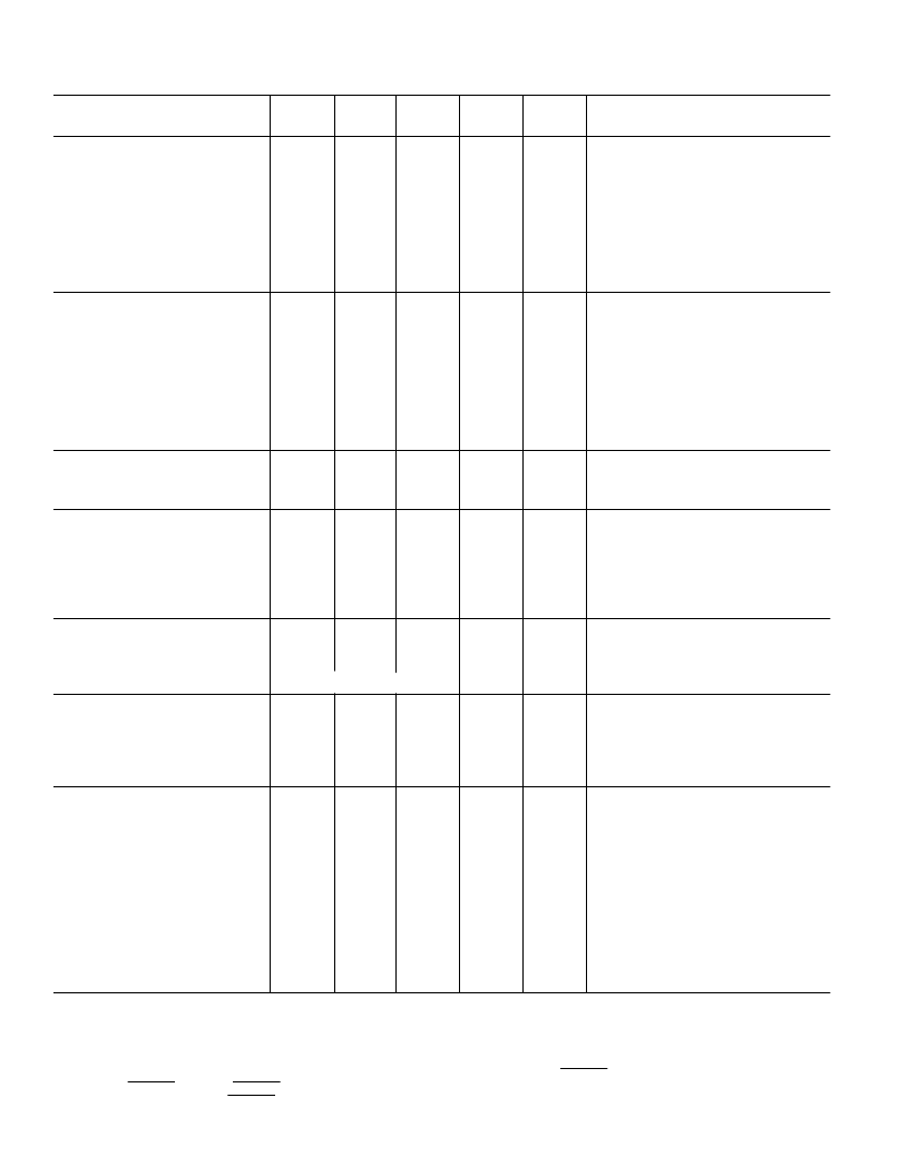
A
Versions
1
Versions
B
J
Version
S
Version
Parameter
Units
Test Conditions/Comments
DYNAMIC PERFORMANCE
2
Signal to (Noise + Distortion) Ratio
3
@ +25
°
C
T
MIN
to T
MAX
Total Harmonic Distortion (THD)
3
Peak Harmonic or Spurious Noise
3
Intermodulation Distortion (IMD)
3
2nd Order Terms
3rd Order Terms
70
70
70
–80
–80
70 typ
70
dB min
dB min
dB max
dB max
f
IN
=10 kHz Sine Wave, f
SAMPLE
= 100 kHz
–80
–80
–80 typ
–80 typ
–80
f
IN
= 10 kHz Sine Wave, f
SAMPLE
= 100 kHz
f
IN
= 10 kHz Sine Wave, f
SAMPLE
= 100 kHz
fa = 9 kHz, fb = 9.5 kHz, f
SAMPLE
= 100 kHz
–80
–80
–80
–80
–80 typ
–80 typ
–80
–80
dB max
dB max
DC ACCURACY
Resolution
Minimum Resolution for which No
Missing Codes are Guaranteed
Relative Accuracy
3
Differential Nonlinearity
3
Positive Full-Scale Error
3
Unipolar Offset Error
12
12
12
12
Bits
12
±
1
±
1
±
3
±
4
±
4
12
±
1/2
±
1
±
1.5
±
4
±
3
12
±
1
±
1
±
3
±
5
±
5
12
±
1
±
1
±
3
±
4
±
4
Bits
LSB max
LSB max
LSB max
LSB max
LSB max
V
DD
= 5 V
±
10%
V
DD
= 2.7 V to 3.6 V
ANALOG INPUT
Input Voltage Range
Input Current
0 to +V
DD
0 to +V
DD
0 to +V
DD
0 to +V
DD
Volts
±
2
±
2
±
2
±
5
μ
A max
LOGIC INPUTS
Input High Voltage, V
INH
2.0
2.4
0.8
±
10
10
2.0
2.4
0.8
±
10
10
2.0
2.4
0.8
±
10
10
2.0
2.4
0.8
±
10
10
V min
V
DD
= 2.7 V to 3.6 V
V
DD
= 5 V
±
10%
Input Low Voltage, V
INL
Input Current, I
IN
Input Capacitance, C
IN4
V max
μ
A max
pF max
V
IN
= 0 V to V
DD
LOGIC OUTPUTS
Output High Voltage, V
OH
Output Low Voltage, V
OL
Output Coding
2.4
0.4
Straight (Natural) Binary
2.4
0.4
2.4
0.4
2.4
0.4
V min
V max
I
SOURCE
= 2 mA
I
SINK
= 2 mA
CONVERSION RATE
Conversion Time:
Mode 1 Operation
Mode 2 Operation
5
Track/Hold Acquisition Time
3
8
14
1.5
8
14
1.5
8
14
1.5
8.5
14.5
1.5
μ
s max
μ
s max
μ
s max
POWER REQUIREMENTS
V
DD
I
DD
+2.7/+5.5 +2.7/+5.5 +2.7/+5.5 +2.7/+5.5 V min/max
4
4
4
4
mA max
Digital Input @ DGND, V
DD
= 2.7 V to
3.6 V
Digital Inputs @ DGND, V
DD
= 5 V
±
10%
V
DD
= 2.7 V, Typically 9 mW
Digital Inputs @ DGND
V
DD
= 2.7 V to 3.6 V
V
DD
= 2.7 V to 3.6 V
V
DD
= 5 V
±
10%
V
DD
= 5 V
±
10%
V
DD
= 2.7 V
5
10.8
5
10.8
5
10.8
5
10.8
mA max
mW max
Power Dissipation
Power-Down Mode
I
DD
@ +25
°
C
T
MIN
to T
MAX
I
DD
@ +25
°
C
T
MIN
to T
MAX
Power Dissipation @ +25
°
C
5
15
50
150
13.5
5
15
50
150
13.5
5
μ
A typ
75
50
500
13.5
5
75
50
500
13.5
μ
A max
μ
A max
μ
A max
μ
A max
μ
W max
NOTES
1
Temperature ranges are as follows: A, B Versions: –40
°
C to +85
°
C; J Version: 0
°
C to +70
°
C; S Version: –55
°
C to +125
°
C.
2
Applies to Mode 1 operation. See section on operating modes.
3
See Terminology.
4
Sample tested @ +25
°
C to ensure compliance.
5
This 14
μ
s includes the “wake-up” time from standby. This “wake-up” time is timed from the rising edge of
CONVST
, whereas conversion is timed from the
falling edge of
CONVST
, for narrow
CONVST
pulse width the conversion time is effectively the “wake-up” time plus conversion time hence 14
μ
s. This can be
seen from Figure 3. Note that if the
CONVST
pulse width is greater than 6
μ
s then the effective conversion time will increase beyond 14
μ
s.
Specifications subject to change without notice.
REV. B
–2–
(V
DD
=
+2.7 V to +5.5 V, AGND = DGND = 0 V. All specifications T
MIN
to T
MAX
unless otherwise noted)
AD7896–SPECIFICATIONS
相關(guān)PDF資料 |
PDF描述 |
|---|---|
| AD7896* | Parallel Input, 12-Bit Rail-to-Rail Micropower DACs in SSOP; Package: PDIP; No of Pins: 24; Temperature Range: -40°C to +85°C |
| AD7898 | 5 V, 12-Bit, Serial 220 kSPS ADC in an 8-Lead Package |
| AD7898AR-10 | 5 V, 12-Bit, Serial 220 kSPS ADC in an 8-Lead Package |
| AD7898AR-3 | 5 V, 12-Bit, Serial 220 kSPS ADC in an 8-Lead Package |
| AD7899 | Evaluation Board for 5V, 12-Bit, Serial 220kSPS ADC in 8-Pin Package |
相關(guān)代理商/技術(shù)參數(shù) |
參數(shù)描述 |
|---|---|
| AD7898AR10 | 制造商:AD 功能描述:New |
| AD7898AR-10 | 功能描述:IC ADC 12BIT SRL HS 5V 8-SOIC RoHS:否 類別:集成電路 (IC) >> 數(shù)據(jù)采集 - 模數(shù)轉(zhuǎn)換器 系列:- 標(biāo)準(zhǔn)包裝:1,000 系列:- 位數(shù):12 采樣率(每秒):300k 數(shù)據(jù)接口:并聯(lián) 轉(zhuǎn)換器數(shù)目:1 功率耗散(最大):75mW 電壓電源:單電源 工作溫度:0°C ~ 70°C 安裝類型:表面貼裝 封裝/外殼:24-SOIC(0.295",7.50mm 寬) 供應(yīng)商設(shè)備封裝:24-SOIC 包裝:帶卷 (TR) 輸入數(shù)目和類型:1 個(gè)單端,單極;1 個(gè)單端,雙極 |
| AD7898AR-10 | 制造商:Analog Devices 功能描述:A/D CONVERTER (A-D) IC ((NW)) |
| AD7898AR-10REEL | 制造商:Analog Devices 功能描述:ADC Single SAR 220ksps 12-bit Serial 8-Pin SOIC N T/R 制造商:Rochester Electronics LLC 功能描述:5V 12-BIT SERIAL ADC IN 8-PIN PKG I.C. - Tape and Reel |
| AD7898AR-10REEL7 | 功能描述:IC ADC 12BIT SRL HS 5V 8-SOIC RoHS:否 類別:集成電路 (IC) >> 數(shù)據(jù)采集 - 模數(shù)轉(zhuǎn)換器 系列:- 標(biāo)準(zhǔn)包裝:1,000 系列:- 位數(shù):16 采樣率(每秒):45k 數(shù)據(jù)接口:串行 轉(zhuǎn)換器數(shù)目:2 功率耗散(最大):315mW 電壓電源:模擬和數(shù)字 工作溫度:0°C ~ 70°C 安裝類型:表面貼裝 封裝/外殼:28-SOIC(0.295",7.50mm 寬) 供應(yīng)商設(shè)備封裝:28-SOIC W 包裝:帶卷 (TR) 輸入數(shù)目和類型:2 個(gè)單端,單極 |
發(fā)布緊急采購(gòu),3分鐘左右您將得到回復(fù)。