- 您現(xiàn)在的位置:買賣IC網(wǎng) > PDF目錄373925 > AD7896SQ (ANALOG DEVICES INC) 2.7 V to 5.5 V, 12-Bit, 8 us ADC in 8-Pin SO/DIP PDF資料下載
參數(shù)資料
| 型號(hào): | AD7896SQ |
| 廠商: | ANALOG DEVICES INC |
| 元件分類: | ADC |
| 英文描述: | 2.7 V to 5.5 V, 12-Bit, 8 us ADC in 8-Pin SO/DIP |
| 中文描述: | 1-CH 12-BIT SUCCESSIVE APPROXIMATION ADC, SERIAL ACCESS, CDIP8 |
| 封裝: | 0.300 INCH, HERMETIC SEALED, CERDIP-8 |
| 文件頁數(shù): | 3/12頁 |
| 文件大小: | 367K |
| 代理商: | AD7896SQ |
AD7896
REV. B
–3–
A, B
Versions
J
Version
S
Version
Parameter
Units
Test Conditions/Comments
t
1
t
2
t
3
t
4
40
40
2
40
2
40
40
2
40
2
40
45
2
45
2
ns min
ns min
ns min
CONVST
Pulse Width
SCLK High Pulse Width
SCLK Low Pulse Width
Data Access Time After Falling Edge of SCLK
V
DD
= 5 V
±
10%
V
DD
= 2.7 V to +3.6 V
Data Hold Time After Falling Edge of SCLK
Bus Relinquish Time After Falling Edge of SCLK
60
3
100
3
10
50
4
60
3
100
3
10
50
4
70
3
110
3
10
50
4
ns max
ns max
ns min
ns max
t
5
t
6
NOTES
1
Sample tested at +25
°
C to ensure compliance. All input signals are measured with tr = tf = 1 ns (10% to 90% of V
DD
) and timed from a voltage level of +1.4 V.
2
The SCLK maximum frequency is 10 MHz. Care must be taken when interfacing to account for the data access time, t
4
, and the setup time required for the user's
processor. These two times will determine the maximum SCLK frequency that the user's system can operate with. See Serial Interface section for more information.
3
Measured with the load circuit of Figure 1 and defined as the time required for an output to cross 0.8 V or 2.0 V.
4
Derived from the measured time taken by the data outputs to change 0.5 V when loaded with the circuit of Figure 1. The measured number is then extrapolated back
to remove the effects of charging or discharging the 50 pF capacitor. This means that the time, t
6
, quoted in the timing characteristics is the true bus relinquish time
of the part and as such is independent of external bus loading capacitances.
TIMING CHARACTERISTICS
1
(V
DD
= +2.7 V to +5.5 V, AGND = DGND = 0 V)
ABSOLUTE MAXIMUM RATINGS*
(T
A
= +25
°
C unless otherwise noted)
V
DD
to AGND . . . . . . . . . . . . . . . . . . . . . . . . . . –0.3 V to +7 V
V
DD
to DGND. . . . . . . . . . . . . . . . . . . . . . . . . . –0.3 V to +7 V
Analog Input Voltage to AGND . . . . . . –0.3 V to V
DD
+ 0.3 V
Digital Input Voltage to DGND . . . . . . –0.3 V to V
DD
+ 0.3 V
Digital Output Voltage to DGND . . . . . –0.3 V to V
DD
+ 0.3 V
Operating Temperature Range
Commercial (J Version) . . . . . . . . . . . . . . . . . 0
°
C to +70
°
C
Industrial (A, B Versions) . . . . . . . . . . . . . . .–40
°
C to +85
°
C
Extended (S Version) . . . . . . . . . . . . . . . . .–55
°
C to +125
°
C
Storage Temperature Range . . . . . . . . . . . . .–65
°
C to +150
°
C
Junction Temperature . . . . . . . . . . . . . . . . . . . . . . . . . +150
°
C
Plastic DIP Package, Power Dissipation . . . . . . . . . . .450 mW
θ
JA
Thermal Impedance . . . . . . . . . . . . . . . . . . . . . 125
°
C/W
θ
JC
Thermal Impedance. . . . . . . . . . . . . . . . . . . . . . 50
°
C/W
Lead Temperature (Soldering, 10 sec) . . . . . . . . . . . +260
°
C
SOIC Package, Power Dissipation . . . . . . . . . . . . . . . .450 mW
θ
JA
Thermal Impedance . . . . . . . . . . . . . . . . . . . . . 160
°
C/W
θ
JC
Thermal Impedance . . . . . . . . . . . . . . . . . . . . . . 75
°
C/W
Lead Temperature, Soldering
Vapor Phase (60 sec) . . . . . . . . . . . . . . . . . . . . . . +215
°
C
Infrared (15 sec) . . . . . . . . . . . . . . . . . . . . . . . . . . +220
°
C
ESD . . . . . . . . . . . . . . . . . . . . . . . . . . . . . . . . . . . . . . .>4000 V
*Stresses above those listed under “Absolute Maximum Ratings” may cause
permanent damage to the device. This is a stress rating only and functional
operation of the device at these or any other conditions above those listed in the
operational sections of this specification is not implied. Exposure to absolute
maximum rating conditions for extended periods may affect device reliability.
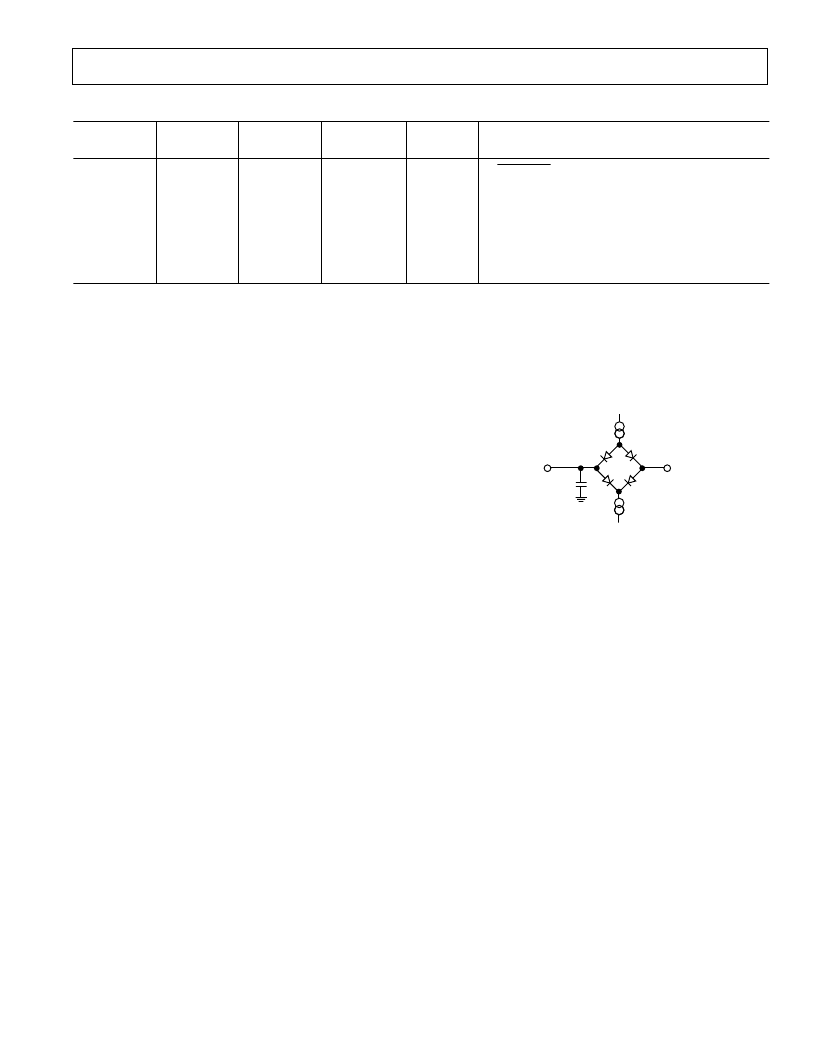
+1.6V
2.0mA
2.0mA
50pF
TO
OUTPUT
PIN
Figure 1. Load Circuit for Access Time and Bus Relinquish
Time
相關(guān)PDF資料 |
PDF描述 |
|---|---|
| AD7896* | Parallel Input, 12-Bit Rail-to-Rail Micropower DACs in SSOP; Package: PDIP; No of Pins: 24; Temperature Range: -40°C to +85°C |
| AD7898 | 5 V, 12-Bit, Serial 220 kSPS ADC in an 8-Lead Package |
| AD7898AR-10 | 5 V, 12-Bit, Serial 220 kSPS ADC in an 8-Lead Package |
| AD7898AR-3 | 5 V, 12-Bit, Serial 220 kSPS ADC in an 8-Lead Package |
| AD7899 | Evaluation Board for 5V, 12-Bit, Serial 220kSPS ADC in 8-Pin Package |
相關(guān)代理商/技術(shù)參數(shù) |
參數(shù)描述 |
|---|---|
| AD7898AR10 | 制造商:AD 功能描述:New |
| AD7898AR-10 | 功能描述:IC ADC 12BIT SRL HS 5V 8-SOIC RoHS:否 類別:集成電路 (IC) >> 數(shù)據(jù)采集 - 模數(shù)轉(zhuǎn)換器 系列:- 標(biāo)準(zhǔn)包裝:1,000 系列:- 位數(shù):12 采樣率(每秒):300k 數(shù)據(jù)接口:并聯(lián) 轉(zhuǎn)換器數(shù)目:1 功率耗散(最大):75mW 電壓電源:單電源 工作溫度:0°C ~ 70°C 安裝類型:表面貼裝 封裝/外殼:24-SOIC(0.295",7.50mm 寬) 供應(yīng)商設(shè)備封裝:24-SOIC 包裝:帶卷 (TR) 輸入數(shù)目和類型:1 個(gè)單端,單極;1 個(gè)單端,雙極 |
| AD7898AR-10 | 制造商:Analog Devices 功能描述:A/D CONVERTER (A-D) IC ((NW)) |
| AD7898AR-10REEL | 制造商:Analog Devices 功能描述:ADC Single SAR 220ksps 12-bit Serial 8-Pin SOIC N T/R 制造商:Rochester Electronics LLC 功能描述:5V 12-BIT SERIAL ADC IN 8-PIN PKG I.C. - Tape and Reel |
| AD7898AR-10REEL7 | 功能描述:IC ADC 12BIT SRL HS 5V 8-SOIC RoHS:否 類別:集成電路 (IC) >> 數(shù)據(jù)采集 - 模數(shù)轉(zhuǎn)換器 系列:- 標(biāo)準(zhǔn)包裝:1,000 系列:- 位數(shù):16 采樣率(每秒):45k 數(shù)據(jù)接口:串行 轉(zhuǎn)換器數(shù)目:2 功率耗散(最大):315mW 電壓電源:模擬和數(shù)字 工作溫度:0°C ~ 70°C 安裝類型:表面貼裝 封裝/外殼:28-SOIC(0.295",7.50mm 寬) 供應(yīng)商設(shè)備封裝:28-SOIC W 包裝:帶卷 (TR) 輸入數(shù)目和類型:2 個(gè)單端,單極 |
發(fā)布緊急采購,3分鐘左右您將得到回復(fù)。