- 您現在的位置:買賣IC網 > PDF目錄373925 > AD7896SQ (ANALOG DEVICES INC) 2.7 V to 5.5 V, 12-Bit, 8 us ADC in 8-Pin SO/DIP PDF資料下載
參數資料
| 型號: | AD7896SQ |
| 廠商: | ANALOG DEVICES INC |
| 元件分類: | ADC |
| 英文描述: | 2.7 V to 5.5 V, 12-Bit, 8 us ADC in 8-Pin SO/DIP |
| 中文描述: | 1-CH 12-BIT SUCCESSIVE APPROXIMATION ADC, SERIAL ACCESS, CDIP8 |
| 封裝: | 0.300 INCH, HERMETIC SEALED, CERDIP-8 |
| 文件頁數: | 9/12頁 |
| 文件大小: | 367K |
| 代理商: | AD7896SQ |
AD7896
REV. B
–9–
The BUSY line can be connected to the
IRQ
line of the
68HC11/L11 if an interrupt driven system is preferred. These
two options are shown in the diagram.
The serial clock rate from the 68HC11/L11 is limited to signifi-
cantly less than the allowable input serial clock frequency with
which the AD7896 can operate. As a result, the time to read
data from the part will actually be longer than the conversion
time of the part. This means that the AD7896 cannot run at its
maximum throughput rate when used with the 68HC11/L11.
AD7896
SDATA
SCLK
BUSY
SCK
MISO
68HC11/L11
PC2 OR
IRQ
Figure 6. AD7896 to 68HC11/L11 Interface
AD7896–ADSP-2103/ADSP-2105 Interface
An interface circuit between the AD7896 and the ADSP-2103/
ADSP-2105 DSP processor is shown in Figure 7. In the inter-
face shown, the RFS1 output from the ADSP-2103/ADSP-
2105s SPORT1 serial port is used to gate the serial clock
(SCLK1) of the ADSP-2103/ADSP-2105 before it is applied to
the SCLK input of the AD7896. The RFS1 output is config-
ured for active high operation. The BUSY line from the
AD7896 is connected to the
IRQ2
line of the ADSP-2103/
ADSP-2105 so that at the end of conversion an interrupt is gen-
erated telling the ADSP-2103/ADSP-2105 to initiate a read op-
eration. The interface ensures a noncontinuous clock for the
AD7896’s serial clock input, with only sixteen serial clock pulses
provided and the serial clock line of the AD7896 remaining low
between data transfers. The SDATA line from the AD7896 is
connected to the DR1 line of the ADSP-2103/ADSP-2105’s
serial port.
The timing relationship between the SCLK1 and RFS1 outputs
of the ADSP-2103/ADSP-2105 are such that the delay between
the rising edge of the SCLK1 and the rising edge of an active
high RFS1 is up to 30 ns. There is also a requirement that data
must be set up 10 ns prior to the falling edge of the SCLK1 to
be read correctly by the ADSP-2103/ADSP-2105. The data ac-
cess time for the AD7896 is 60 ns (5 V (A, B versions)) from
the rising edge of its SCLK input. Assuming a 10 ns propaga-
tion delay through the external AND gate, the high time of the
SCLK1 output of the ADSP-2105 must be
≥
(30 + 60 +10
+10) ns, i.e.,
≥
110 ns. This means that the serial clock fre-
quency with which the interface of Figure 7 can work is limited
to 4.5 MHz. However, there is an alternative method which al-
lows for the ADSP-2105 SCLK1 to run at 5 MHz (which is the
max serial clock frequency of the SCLK1 output). The arrange-
ment is where the first leading zero of the data stream from the
AD7896 cannot be guaranteed to be clocked into the ADSP-
2105 due to the combined delay of the RFS signal and the data
access time of the AD7896. In most cases this is acceptable as
there will still be three leading zeros followed by the 12 data
bits. For the ADSP-2103 the SCLK1 frequency will need to be
limited to < 4 MHz to account for the 100 ns data access time
of the AD7896 at 3 V.
To chip select the AD7896 in systems where more than one de-
vice is connected to the 8X51/L51’s serial port, a port bit, con-
figured as an output, from one of the 8X51/L51’s parallel ports
can be used to gate on or off the serial clock to the AD7896. A
simple AND function on this port bit and the serial clock from
the 8X51/L51 will provide this function. The port bit should be
high to select the AD7896 and low when it is not selected.
The end of conversion is monitored by using the BUSY signal
which is shown in the interface diagram of Figure 5. With the
BUSY line from the AD7896 connected to the Port P1.2 of the
8X51/L51 so the BUSY line can be polled by the 8X51/L51.
The BUSY line can be connected to the INT1 line of the 8X51/
L51 if an interrupt driven system is preferred. These two op-
tions are shown on the diagram.
Note also that the AD7896 outputs the MSB first during a read
operation while the 8X51/L51 expects the LSB first. Therefore,
the data which is read into the serial buffer needs to be rear-
ranged before the correct data format from the AD7896 appears
in the accumulator.
The serial clock rate from the 8X51/L51 is limited to signifi-
cantly less than the allowable input serial clock frequency with
which the AD7896 can operate. As a result, the time to read
data from the part will actually be longer than the conversion
time of the part. This means that the AD7896 cannot run at its
maximum throughput rate when used with the 8X51/L51.
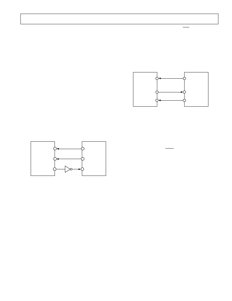
AD7896
SDATA
SCLK
BUSY
P3.0
P3.1
8X51/L51
P1.2
OR
INT1
Figure 5. AD7896 to 8X51/L51 Interface
AD7896–68HC11/L11 Interface
An interface circuit between the AD7896 and the 68HC11/L11
microcontroller is shown in Figure 6. For the interface shown,
the 68HC11/L11 SPI port is used and the 68HC11/L11 is con-
figured in its single-chip mode. The 68HC11/L11 is configured
in the master mode with its CPOL bit set to a logic zero and its
CPHA bit set to a logic one. As with the previous interface, the
diagram shows the simplest form of the interface where the
AD7896 is the only part connected to the serial port of the
68HC11/L11 and, therefore, no decoding of the serial read
operations is required.
Once again, to chip select the AD7896 in systems where more
than one device is connected to the 68HC11/L11’s serial port, a
port bit, configured as an output, from one of the 68HC11/
L11’s parallel ports can be used to gate on or off the serial clock
to the AD7896. A simple AND function on this port bit and
the serial clock from the 68HC11/L11 will provide this function.
The port bit should be high to select the AD7896 and low when
it is not selected.
The end of conversion is monitored by using the BUSY signal
which is shown in the interface diagram of Figure 6. With the
BUSY line from the AD7896 connected to the Port PC0 of the
68HC11/L11 the BUSY line can be polled by the 68HC11/L11.
相關PDF資料 |
PDF描述 |
|---|---|
| AD7896* | Parallel Input, 12-Bit Rail-to-Rail Micropower DACs in SSOP; Package: PDIP; No of Pins: 24; Temperature Range: -40°C to +85°C |
| AD7898 | 5 V, 12-Bit, Serial 220 kSPS ADC in an 8-Lead Package |
| AD7898AR-10 | 5 V, 12-Bit, Serial 220 kSPS ADC in an 8-Lead Package |
| AD7898AR-3 | 5 V, 12-Bit, Serial 220 kSPS ADC in an 8-Lead Package |
| AD7899 | Evaluation Board for 5V, 12-Bit, Serial 220kSPS ADC in 8-Pin Package |
相關代理商/技術參數 |
參數描述 |
|---|---|
| AD7898AR10 | 制造商:AD 功能描述:New |
| AD7898AR-10 | 功能描述:IC ADC 12BIT SRL HS 5V 8-SOIC RoHS:否 類別:集成電路 (IC) >> 數據采集 - 模數轉換器 系列:- 標準包裝:1,000 系列:- 位數:12 采樣率(每秒):300k 數據接口:并聯 轉換器數目:1 功率耗散(最大):75mW 電壓電源:單電源 工作溫度:0°C ~ 70°C 安裝類型:表面貼裝 封裝/外殼:24-SOIC(0.295",7.50mm 寬) 供應商設備封裝:24-SOIC 包裝:帶卷 (TR) 輸入數目和類型:1 個單端,單極;1 個單端,雙極 |
| AD7898AR-10 | 制造商:Analog Devices 功能描述:A/D CONVERTER (A-D) IC ((NW)) |
| AD7898AR-10REEL | 制造商:Analog Devices 功能描述:ADC Single SAR 220ksps 12-bit Serial 8-Pin SOIC N T/R 制造商:Rochester Electronics LLC 功能描述:5V 12-BIT SERIAL ADC IN 8-PIN PKG I.C. - Tape and Reel |
| AD7898AR-10REEL7 | 功能描述:IC ADC 12BIT SRL HS 5V 8-SOIC RoHS:否 類別:集成電路 (IC) >> 數據采集 - 模數轉換器 系列:- 標準包裝:1,000 系列:- 位數:16 采樣率(每秒):45k 數據接口:串行 轉換器數目:2 功率耗散(最大):315mW 電壓電源:模擬和數字 工作溫度:0°C ~ 70°C 安裝類型:表面貼裝 封裝/外殼:28-SOIC(0.295",7.50mm 寬) 供應商設備封裝:28-SOIC W 包裝:帶卷 (TR) 輸入數目和類型:2 個單端,單極 |
發布緊急采購,3分鐘左右您將得到回復。