- 您現在的位置:買賣IC網 > PDF目錄373929 > AD8018 (Analog Devices, Inc.) RESISTOR-FIXED, METAL PDF資料下載
參數資料
| 型號: | AD8018 |
| 廠商: | Analog Devices, Inc. |
| 英文描述: | RESISTOR-FIXED, METAL |
| 中文描述: | 5伏,軌到軌,高輸出電流,xDSL線路驅動器放大器 |
| 文件頁數: | 9/19頁 |
| 文件大小: | 339K |
| 代理商: | AD8018 |
REV. 0
AD8018
–9–
Table I. Resistor Selection Guide
Gain
R
F
( )
681
1 k
750
511
340
230
R
G
( )
681
∞
750
256
113
59
–
1
+1
+2
+3
+4
+5
POWER-DOWN FEATURES
Two digitally programmable logic pins, PWDN1 and PWDN0,
are available on the TSSOP-14 package to select among three
different modes of operation, full power, standby and shutdown.
The DGND pin is the logic ground reference. The logic thresh-
old voltage is established 1 V above DGND. In a typical 5 V
single-supply application, the DGND pin is connected to analog
ground. If PWDN1, PWDN0, and DGND are left unconnected,
the AD8018 will operate at full power.
Table II. Power-Down Features and Truth Table
Supply
Current
Output
Impedance
PWDN0
PWDN1
State
High
Low
High
Low
High
High
Low
Low
Full Power
Standby
Standby
Disabled
18 mA
9 mA
9 mA
300
μ
A
Low
Low
Low
High
POWER SUPPLY AND DECOUPLING
The AD8018 can be powered with a good quality (i.e., low-noise)
supply anywhere in the range from 3.3 V to 8 V. However, in
order to optimize the ADSL upstream drive capability to +13 dBm
and maintain the best Spurious Free Dynamic Range (SFDR),
the AD8018 circuit should be supplied with a well regulated 5 V
supply. The 5 V supplied at the USB port may be poorly regu-
lated. Improving the quality of the 5 V supply will optimize the
performance of the AD8018 in a USB-supplied CPE ADSL
modem. This can be accomplished through the use of a step-up
dc-to-dc converter or switching power supply followed by a low
dropout (LDO) regulator such as the ADP3331 (see Figure 6).
Setting R1 to be 953 k
and R2 to be 301 k
will result in a
V
OUT
of 5 V.
Careful attention must be paid to decoupling the power supply
pins at the output of the dc-to-dc converter, the output of the
LDO regulator and the supply pins of the AD8018. High-quality
capacitors with low equivalent series resistance (ESR) such as
multilayer ceramic capacitors (MLCCs) should be used to mini-
mize supply voltage ripple and power dissipation. A large, usually
tantalum, 10
μ
F to 47
μ
F capacitor located in proximity to the
AD8018 is required to provide good decoupling for lower fre-
quency signals. In addition, 0.1
μ
F MLCC decoupling capacitors
should be located as close to each of the power supply pins as is
physically possible, no more than 1/8 inch away. An additional
large (4.7
μ
F to 10
μ
F) tantalum capacitor should be placed on the
board near the supply terminals to supply current for fast, large-
signal changes at the AD8018 outputs.
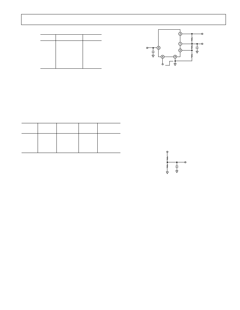
ADP3331
C1
0.47 F
V
IN
ON
OFF
V
OUT
E
OUT
C2
0.47 F
R3
330k
IN
SD
GND
OUT
FB
ERR
R1
953k
R2
301k
Figure 6. ADP3331 LDO
METHOD FOR GENERATING A MIDSUPPLY VOLTAGE
To operate an amplifier on a single voltage supply, a voltage
midway between the supply and ground must be generated to
properly bias the inputs and the outputs.
A voltage divider can be created with two equal value resistors
(Figure 7). There is a trade-off between the power consumed by
the divider and the voltage drop across these resistors due to the
positive input bias currents. Selecting 2.5 k
for R1 and R2 will
create a voltage divider that draws only 1 mA from a 5 V supply.
The voltage generated with this topology can vary due to the
temperature coefficient (TC) of resistance. Resistors that are
closely matched and have a low TC will minimize variations in
the voltage reference due to temperature. One should also be
sure to use a decoupling capacitor (0.1
μ
F) at the node where
V
REF
is generated.
5V
R1
2.5k
R2
2.5k
V
REF
0.1 F
Figure 7. Midsupply Reference
DIFFERENTIAL TESTING
The test circuit shown in TPC 13 is used for measuring the dif-
ferential distortion of the AD8018. A single-ended test signal is
applied to the inverting input of the AD8138 differential driver
with the noninverting input grounded. Applying the differential
output of the AD8138 through 100
resistors serves to isolate
the inputs of the AD8018 differential driver and provide a well-
balanced low-distortion input signal. The differential load (R
L
)
of the AD8018 can be set to the equivalent of the line imped-
ance reflected through a transformer. The AD9632 converts
the differential output voltage back to a single-ended signal.
The differential-to- single-ended converter using the AD9632
has an attenuation of
–
26 dB and is wired with precision resis-
tors to optimize the balance of differential input signal. The
resulting smaller output signal can be easily measured using a
50
spectrum analyzer.
相關PDF資料 |
PDF描述 |
|---|---|
| AD8018AR | 5 V, Rail-to-Rail, High-Output Current, xDSL Line Drive Amplifier |
| AD8018ARU | 5 V, Rail-to-Rail, High-Output Current, xDSL Line Drive Amplifier |
| AD8018AR-REEL | 5 V, Rail-to-Rail, High-Output Current, xDSL Line Drive Amplifier |
| AD8019ARU-EVAL | DSL Line Driver with Power-Down |
| AD8019ARU-REEL | DSL Line Driver with Power-Down |
相關代理商/技術參數 |
參數描述 |
|---|---|
| AD80182ABSVZ | 制造商:Analog Devices 功能描述: |
| AD80182BSVZ | 制造商:Analog Devices 功能描述: |
| AD80184BBCZ | 制造商:Analog Devices 功能描述: |
| AD80185BBCZ | 制造商:Analog Devices 功能描述: |
| AD8018AR | 制造商:Analog Devices 功能描述:ADSL Driver Dual 8-Pin SOIC N Tube 制造商:Rochester Electronics LLC 功能描述:SOIC DUAL+5V HISPD HI OUTPUT CURRENT AMP - Bulk 制造商:Analog Devices 功能描述:AMP DUAL LINE DRIVER RRO/P 8018 |
發布緊急采購,3分鐘左右您將得到回復。