- 您現在的位置:買賣IC網 > PDF目錄373929 > AD8018ARU (ANALOG DEVICES INC) 5 V, Rail-to-Rail, High-Output Current, xDSL Line Drive Amplifier PDF資料下載
參數資料
| 型號: | AD8018ARU |
| 廠商: | ANALOG DEVICES INC |
| 元件分類: | 運動控制電子 |
| 英文描述: | 5 V, Rail-to-Rail, High-Output Current, xDSL Line Drive Amplifier |
| 中文描述: | DUAL OP-AMP, 17000 uV OFFSET-MAX, PDSO14 |
| 封裝: | PLASTIC, TSSOP-14 |
| 文件頁數: | 10/19頁 |
| 文件大小: | 339K |
| 代理商: | AD8018ARU |
REV. 0
AD8018
–10–
P
V rmsV
V rms
R
I V
P
TOT
S
L
S
OUT
=
×
+
+
4 0 8
( .
1
2
2
–
)
α
For the AD8018, operating on a single 5 V supply and deliver-
ing a total of 16 dBm (13 dBm to the line and 3 dBm to the
matching network) into 12.5
(100
reflected back through
a 1:4.0 transformer plus back termination), the power is:
= 261
mW
+ 40
mW
= 301
mW
Using these calculations, and a
θ
JA
of 115
°
C/W for the TSSOP
package and 100
°
C/W for the SOIC, Tables III and IV show
junction temperature versus power delivered to the line for sev-
eral supply voltages.
Table III. Junction Temperature vs. Line Power and
Operating Voltage for TSSOP, T
AMB
= 85 C
V
SUPPLY
5
P
LINE
13
14
15
16
17
18
6
7
8
115
117
119
121
123
125
122
125
127
130
133
136
129
132
136
139
143
147
136
140
144
148
153
158
Table IV. Junction Temperature vs. Line Power and
Operating Voltage for SOIC, T
AMB
= 85 C
V
SUPPLY
6
P
LINE,
dBm
13
14
15
16
17
18
5
7
8
111
113
115
116
118
120
117
119
122
124
127
130
123
126
129
132
136
139
129
133
136
140
144
149
Running the AD8018 at voltages near 8 V can produce junction
temperatures that exceed the thermal rating of the TSSOP pack-
ages and should be avoided. The shaded areas indicate junction
temperatures greater than 150
°
C.
LAYOUT CONSIDERATIONS
As is the case with all high-speed applications, careful attention
to printed circuit board layout details will prevent associated
board parasitics from becoming problematic. Proper RF design
technique is mandatory. The PCB should have a ground plane
covering all unused portions of the component side of the board
to provide a low-impedance return path. Removing the ground
plane on all layers from the area near the input and output pins
will reduce stray capacitance, particularly in the area of the
inverting inputs. Signal lines connecting the feedback and gain
resistors should be as short as possible to minimize the inductance
and stray capacitance associated with these traces. Termination
resistors and loads should be located as close as possible to their
respective inputs and outputs. Input and output traces should
be kept as far apart as possible to minimize coupling (crosstalk)
though the board. Adherence to stripline design techniques for
long signal traces (greater than about 1 inch) is recommended.
This circuit requires significant power supply bypassing. The
AD8018 operates on a split supply in this circuit. The bypassing
technique shown in TPC 13 utilizes a 220
μ
F tantalum capacitor
and a 0.1
μ
F ceramic chip capacitor in parallel, connected from
the positive to negative supply, and a 10
μ
F tantalum and 0.1
μ
F
ceramic chip capacitor in parallel, connected from each supply to
ground. The capacitors connected between the power supplies
serve to minimize any voltage ripples that might appear at the
supplies while sourcing or sinking any large differential current.
The large capacitor has a pool of charge instantly available for
the AD8018 to draw from, thus preventing any erroneous dis-
tortion results.
POWER DISSIPATION
It is important to consider the total power dissipation of the
AD8018 in order to properly size the heat sink area of an
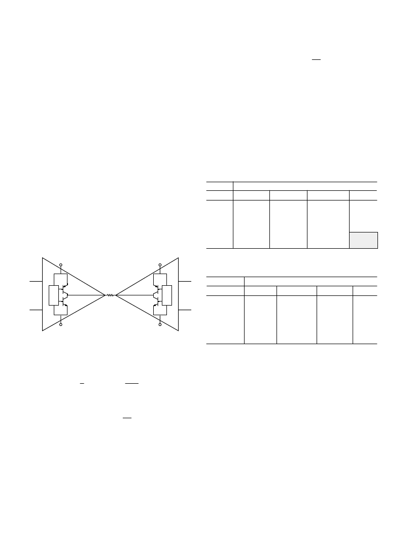
application. Figure 8 is a simple representation of a differential
driver. With some simplifying assumptions we can estimate the
total power dissipated in this circuit. If the output current is
large compared to the quiescent current, computing the dissipa-
tion in the output devices and adding it to the quiescent power
dissipation will give a close approximation of the total power
dissipation in the package. A factor
α
(~0.6-1) corrects for the
slight error due to the Class A/B operation of the output stage.
It can be estimated by subtracting the quiescent current in the
output stage from the total quiescent current and ratioing that
to the total quiescent current. For the AD8018,
α
= 0.833.
+V
S
–
V
S
+V
O
+V
S
–
V
S
–
V
O
R
L
Figure 8. Simplified Differential Driver
Remembering that each output device dissipates for only half
the time gives a simple integral that computes the power for
each device:
1
2
2
∫
×
(
–
)
V
V
V
R
S
O
O
L
The total supply power can then be computed as:
P
V
V
|
V
R
I V
P
TOT
S
O
O
L
S
OUT
=
∫
∫
+
+
4
1
2
2
|
α
In this differential driver, V
O
is the voltage at the output of one
amplifier, so 2
V
O
is the voltage across
R
L
,
which is the total
impedance seen by the differential driver,
including back ter-
mination.
Now, with two observations, the integrals are easily
evaluated. First, the integral of V
O2
is simply the square of the
rms value of V
O
. Second, the integral of |V
O
| is equal to the
average rectified value of V
O
, sometimes called the Mean Aver-
age Deviation, or MAD. It can be shown that for a DMT signal,
the MAD value is equal to 0.8 times the rms value.
相關PDF資料 |
PDF描述 |
|---|---|
| AD8018AR-REEL | 5 V, Rail-to-Rail, High-Output Current, xDSL Line Drive Amplifier |
| AD8019ARU-EVAL | DSL Line Driver with Power-Down |
| AD8019ARU-REEL | DSL Line Driver with Power-Down |
| AD8019 | DSL Line Driver with Power-Down |
| AD8019AR | DSL Line Driver with Power-Down |
相關代理商/技術參數 |
參數描述 |
|---|---|
| AD8018ARU-EVAL | 功能描述:BOARD EVAL FOR AD8018 RoHS:否 類別:編程器,開發系統 >> 評估演示板和套件 系列:- 標準包裝:1 系列:- 主要目的:電信,線路接口單元(LIU) 嵌入式:- 已用 IC / 零件:IDT82V2081 主要屬性:T1/J1/E1 LIU 次要屬性:- 已供物品:板,電源,線纜,CD 其它名稱:82EBV2081 |
| AD8018ARU-REEL | 制造商:Analog Devices 功能描述:ADSL Driver Dual 14-Pin TSSOP T/R 制造商:Rochester Electronics LLC 功能描述:TSSOP DUAL+5V HISPD HIOUTPUTCURRENT AMP - Tape and Reel |
| AD8018ARU-REEL7 | 制造商:Analog Devices 功能描述:ADSL Driver Dual 14-Pin TSSOP T/R 制造商:Rochester Electronics LLC 功能描述:TSSOP DUAL+5V HISPD HIOUTPUTCURRENT AMP - Tape and Reel |
| AD8018ARUZ | 功能描述:IC LINE DRIVER XDSL R-R 14TSSOP RoHS:是 類別:集成電路 (IC) >> 接口 - 驅動器,接收器,收發器 系列:- 標準包裝:1 系列:- 類型:線路收發器 驅動器/接收器數:5/3 規程:RS232 電源電壓:3 V ~ 5.5 V 安裝類型:表面貼裝 封裝/外殼:28-SOIC(0.295",7.50mm 寬) 供應商設備封裝:28-SOIC 包裝:Digi-Reel® 產品目錄頁面:918 (CN2011-ZH PDF) 其它名稱:296-25096-6 |
| AD8018ARUZ-REEL | 功能描述:IC LINE DRIVER XDSL R-R 14TSSOP RoHS:是 類別:集成電路 (IC) >> 接口 - 驅動器,接收器,收發器 系列:- 標準包裝:27 系列:- 類型:收發器 驅動器/接收器數:3/3 規程:RS232,RS485 電源電壓:4.75 V ~ 5.25 V 安裝類型:表面貼裝 封裝/外殼:28-SOIC(0.295",7.50mm 寬) 供應商設備封裝:28-SOIC 包裝:管件 |
發布緊急采購,3分鐘左右您將得到回復。