- 您現(xiàn)在的位置:買賣IC網(wǎng) > PDF目錄373942 > AD830 (Analog Devices, Inc.) High Speed, Video Difference Amplifier(高速,視頻差分運放) PDF資料下載
參數(shù)資料
| 型號: | AD830 |
| 廠商: | Analog Devices, Inc. |
| 元件分類: | 運動控制電子 |
| 英文描述: | High Speed, Video Difference Amplifier(高速,視頻差分運放) |
| 中文描述: | 高速,視頻差分放大器(高速,視頻差分運放) |
| 文件頁數(shù): | 9/16頁 |
| 文件大小: | 244K |
| 代理商: | AD830 |
AD830
REV. A
–9–
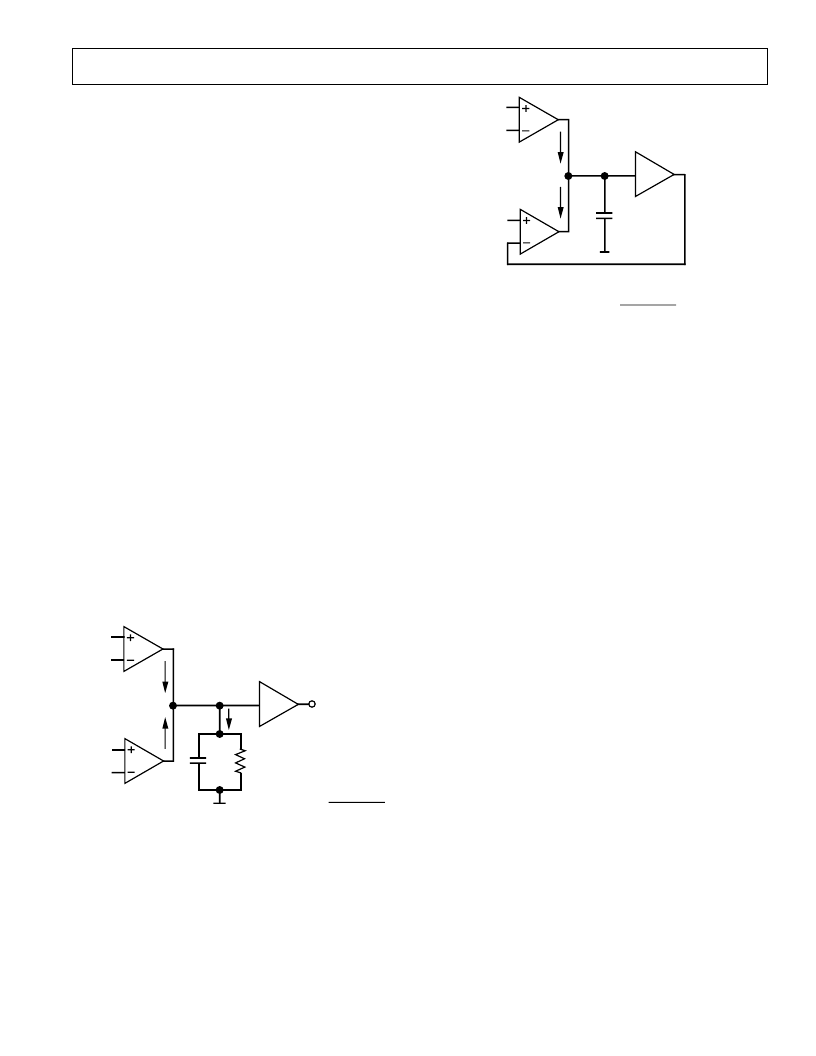
UNDE RST ANDING T HE AD830 T OPOLOGY
T he AD830 represents Analog Devices’ first amplifier product
to embody a powerful alternative amplifier topology. Referred to
as active feedback, the topology used in the AD830 provides in-
herent advantages in the handling of differential signals, differ-
ing system commons, level shifting and low distortion, high
frequency amplification. In addition, it makes possible the
implementation of many functions not realizable with single op
amp circuits or is superior to op amp based equivalent circuits.
With this in mind, it is important to understand the internal
structure of the AD830.
T he topology, reduced to its elemental form, is shown below in
Figure 21. Nonideal effects such as nonlinearity, bias currents
and limited full scale are omitted from this model for simplicity,
but are discussed later. T he key feature of this topology is the
use of two, identical voltage-to-current converters, G
M
, that
make up input and feedback signal interfaces. T hey are labeled
with inputs V
X
and V
Y
, respectively. T hese voltage to current
converters possess fully differential inputs, high linearity, high
input impedance and wide voltage range operation. T his enables
the part to handle large amplitude differential signals; they also
provide high common-mode rejection, low distortion and negli-
gible loading on the source. T he label, G
M
, is meant to convey
that the transconductance is a large signal quantity, unlike in the
front-end of most op amps. T he two G
M
stage current outputs
I
X
and I
Y
, sum together at a high impedance node which is char-
acterized by an equivalent resistance and capacitance connected
to an “ac common.” A unity voltage gain stage follows the high
impedance node to provide buffering from loads. Relative to
either input, the open loop gain, A
OL
, is set by the
transconductance, G
M
, working into the resistance, R
P
; A
OL
=
G
M
3
R
P
. T he unity gain frequency
ω
0
dB
for the open loop gain
is established by the transconductance, G
M
, working into the
capacitance, C
C
;
ω
0
dB
= G
M
/C
C
. T he open loop description of
the AD830 is shown below for completeness.
A=1
V
OUT
V
X2
V
X1
I
X
= (V
X1
– V
X2
) G
M
I
Y
= (V
– V
Y2
) G
M
I
Z
= I
X
+ I
Y
I
Y
I
X
V
Y2
V
Y1
G
M
G
M
I
Z
A
OLS
=
G
M
R
P
1 + S (C
C
R
P
)
C
C
R
P
Figure 21. Topology Diagram
A=1
V
OUT
V
X2
V
X1
V
X1
– V
X2
= V
Y
2
– V
Y1
FOR V
Y2
= V
OUT
V
OUT
= (V
X1
– V
X2
+ V
Y1
)
I
Y
I
X
V
Y2
V
Y1
G
M
G
M
1
1 + S(C
C
/G
M
)
C
C
Figure 22. Closed-Loop Connection
Precise amplification is accomplished through closed-loop op-
eration of this topology. Voltage feedback is implemented via
the Y G
M
stage in which where the output is connected to the
–Y input for negative feedback as shown in Figure 22. An input
signal is applied across the X G
M
stage, either fully differentially
or single-ended referred to common. It produces a current sig-
nal which is summed at the high impedance node with the out-
put current from the Y G
M
stage. Negative feedback nulls this
sum to a small error current necessary to develop the output
voltage at the high impedance node. T he error current is usually
negligible, so the null condition essentially forces the Y G
M
output stage current to exactly equal the X G
M
output current.
Since the two transconductances are identical, the differential
voltage across the Y inputs equals the negative of the differential
voltage across the X input; V
Y
= –V
X
or more precisely
V
Y2
–V
Y1
= V
X 1
–V
X 2
. T his simple relation provides the basis to
easily analyze any function possible to synthesize with the
AD830, including any feedback situation.
T he bandwidth of the circuit is defined by the G
M
and the
capacitor C
C
. T he highly linear G
M
stages give the amplifier a
single pole response, excluding the output amplifier and loading
effects.
It is important to note that the bandwidth and general dy-
namic behavior is symmetrical (identical) for the noninverting
and
the inverting connections of the AD830.
In addition, the input im-
pedance and CMRR are the same for either connections. T his is
very advantageous and unlike in a voltage or current feedback
amplifier, where there is a distinct difference in performance be-
tween the inverting and noninverting gain. T he practical impor-
tance of this cannot be overemphasized and is a key feature
offered by the AD830 amplifier topology.
相關PDF資料 |
PDF描述 |
|---|---|
| AD8313ARM-REEL7 | 0.1 GHz-2.5 GHz, 70 dB Logarithmic Detector/Controller |
| AD8313ARM | 0.1 GHz-2.5 GHz, 70 dB Logarithmic Detector/Controller |
| AD8313ARM-REEL | 0.1 GHz-2.5 GHz, 70 dB Logarithmic Detector/Controller |
| AD8313-EVAL | 0.1 GHz-2.5 GHz, 70 dB Logarithmic Detector/Controller |
| AD8313 | 0.1 GHz-2.5 GHz,70dB Logarithmic Detector/Controller(頻率為0.1 GHz-2.5 GHz,增益為70dB的對數(shù)檢測器/控制器) |
相關代理商/技術(shù)參數(shù) |
參數(shù)描述 |
|---|---|
| AD830_10 | 制造商:AD 制造商全稱:Analog Devices 功能描述:High Speed, Video Difference Amplifier |
| AD8300 | 制造商:AD 制造商全稱:Analog Devices 功能描述:+3 Volt, Serial Input Complete 12-Bit DAC |
| AD8300AN | 功能描述:IC DAC 12-BIT SERIAL 8-DIP RoHS:否 類別:集成電路 (IC) >> 數(shù)據(jù)采集 - 數(shù)模轉(zhuǎn)換器 系列:- 標準包裝:2,400 系列:- 設置時間:- 位數(shù):18 數(shù)據(jù)接口:串行 轉(zhuǎn)換器數(shù)目:3 電壓電源:模擬和數(shù)字 功率耗散(最大):- 工作溫度:-40°C ~ 85°C 安裝類型:表面貼裝 封裝/外殼:36-TFBGA 供應商設備封裝:36-TFBGA 包裝:帶卷 (TR) 輸出數(shù)目和類型:* 采樣率(每秒):* |
| AD8300ANZ | 功能描述:IC DAC 12BIT SERIAL 8DIP RoHS:是 類別:集成電路 (IC) >> 數(shù)據(jù)采集 - 數(shù)模轉(zhuǎn)換器 系列:- 標準包裝:1 系列:- 設置時間:4.5µs 位數(shù):12 數(shù)據(jù)接口:串行,SPI? 轉(zhuǎn)換器數(shù)目:1 電壓電源:單電源 功率耗散(最大):- 工作溫度:-40°C ~ 125°C 安裝類型:表面貼裝 封裝/外殼:8-SOIC(0.154",3.90mm 寬) 供應商設備封裝:8-SOICN 包裝:剪切帶 (CT) 輸出數(shù)目和類型:1 電壓,單極;1 電壓,雙極 采樣率(每秒):* 其它名稱:MCP4921T-E/SNCTMCP4921T-E/SNRCTMCP4921T-E/SNRCT-ND |
| AD8300AR | 功能描述:IC DAC 12BIT 3V SRL-IN 8-SOIC RoHS:否 類別:集成電路 (IC) >> 數(shù)據(jù)采集 - 數(shù)模轉(zhuǎn)換器 系列:- 標準包裝:47 系列:- 設置時間:2µs 位數(shù):14 數(shù)據(jù)接口:并聯(lián) 轉(zhuǎn)換器數(shù)目:1 電壓電源:單電源 功率耗散(最大):55µW 工作溫度:-40°C ~ 85°C 安裝類型:表面貼裝 封裝/外殼:28-SSOP(0.209",5.30mm 寬) 供應商設備封裝:28-SSOP 包裝:管件 輸出數(shù)目和類型:1 電流,單極;1 電流,雙極 采樣率(每秒):* |
發(fā)布緊急采購,3分鐘左右您將得到回復。