- 您現(xiàn)在的位置:買(mǎi)賣(mài)IC網(wǎng) > PDF目錄373944 > AD8343-EVAL (Analog Devices, Inc.) DC-to-2.5 GHz High IP3 Active Mixer PDF資料下載
參數(shù)資料
| 型號(hào): | AD8343-EVAL |
| 廠(chǎng)商: | Analog Devices, Inc. |
| 英文描述: | DC-to-2.5 GHz High IP3 Active Mixer |
| 中文描述: | DC至2.5GHz的高IP3有源混頻器 |
| 文件頁(yè)數(shù): | 13/27頁(yè) |
| 文件大小: | 394K |
| 代理商: | AD8343-EVAL |
第1頁(yè)第2頁(yè)第3頁(yè)第4頁(yè)第5頁(yè)第6頁(yè)第7頁(yè)第8頁(yè)第9頁(yè)第10頁(yè)第11頁(yè)第12頁(yè)當(dāng)前第13頁(yè)第14頁(yè)第15頁(yè)第16頁(yè)第17頁(yè)第18頁(yè)第19頁(yè)第20頁(yè)第21頁(yè)第22頁(yè)第23頁(yè)第24頁(yè)第25頁(yè)第26頁(yè)第27頁(yè)
REV. 0
AD8343
–13–
DC INTERFACES
Biasing and Decoupling (VPOS, DCPL)
VPOS is the power supply connection for the internal bias cir-
cuit and the LO driver. This pin should be closely bypassed to
GND with a capacitor in the range of 0.01
μ
F to 0.1
μ
F. The
DCPL pin provides access to an internal bias node for noise
bypassing purposes. This node should be bypassed to COMM
with 0.1
μ
F.
Power-Down Interface (PWDN)
The AD8343 is active when the PWDN pin is held low; other-
wise the device enters a low-power state as shown in Figure 3.
PWDN SWEPT
FROM BOTH
3V TO 5V
AND
5V TO 3V
PWDN VOLTAGE
–
Volts
0
3.0
3.5
D
–
4.0
4.5
5.0
5
10
15
20
25
30
35
40
45
Figure 3. Bias Current vs. PWDN Voltage
To assure full power-down, the PWDN voltage should be within
0.5 V of the supply voltage at VPOS. Normal operation requires
that the PWDN pin be taken at least 1.5 V below the supply
voltage. The PWDN pin sources about 100
μ
A when pulled to
GND (refer to Pin Function Descriptions). It is not advisable to
leave the pin floating when the device is to be disabled; a resis-
tive pull-up to VPOS is the minimum suggestion.
The AD8343 requires about 2.5
μ
s to turn OFF when PWDN is
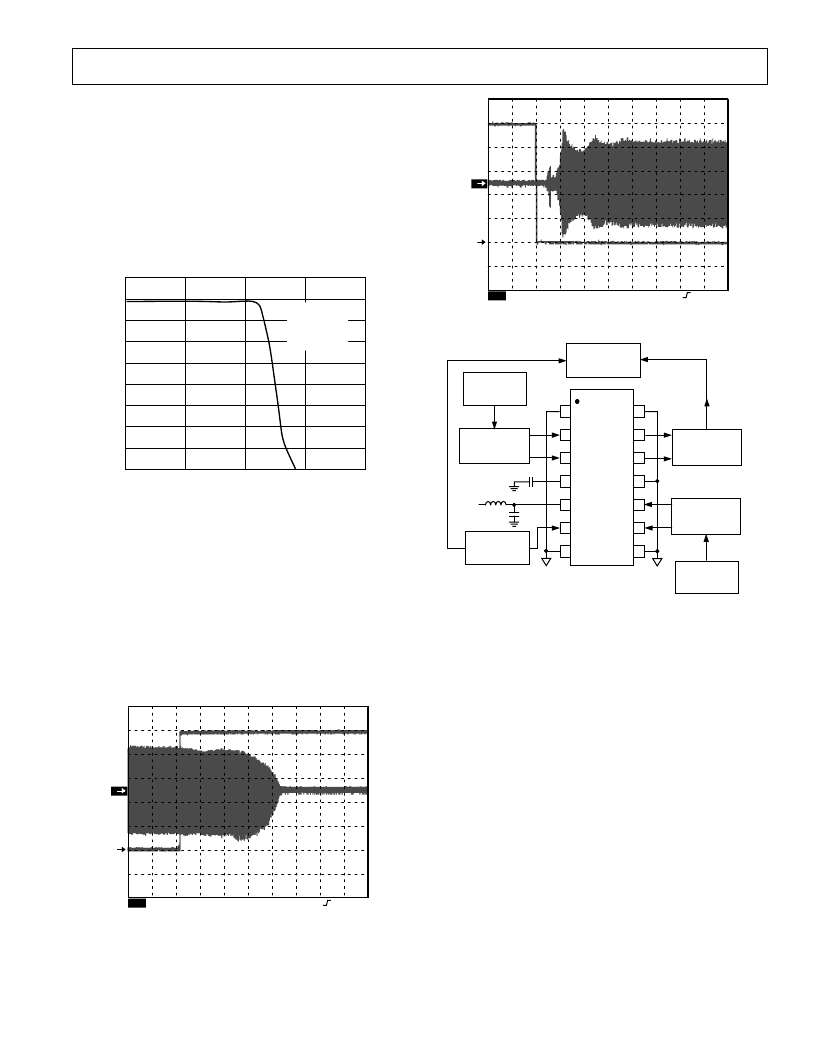
asserted; turn ON time is about 500 ns. Figures 4 and 5 show
typical characteristics (they will vary with bypass component
values). Figure 6 shows the test configuration used to acquire
these waveforms.
2
200nV
1.00V
CH2
M
500ns CH2
4.48V
1
CH1
Figure 4. PWDN Response Time Device ON to OFF
2
200nV
1.00V
CH2
M
100ns CH2
4.48V
1
CH1
Figure 5. PWDN Response Time Device OFF to ON
1nH
0.1 F
VPOS
0.1 F
14
13
12
11
10
9
8
1
2
3
4
5
6
7
COMM
AD8343
INPP
INPM
DCPL
VPOS
PWDN
COMM
COMM
OUTP
OUTM
COMM
LOIP
LOIM
COMM
MATCHING
NETWORK AND
TRANSFORMER
TRANSFORMER
HP8130
PULSE
GENERATOR
HP8648C
SIGNAL
GENERATOR
TEKTRONIX
TDS694C
OSCILLOSCOPE
RF INPUT
1740MHz
IF OUTPUT
170MHz
LO INPUT
1570MHz
MATCHING
NETWORK AND
TRANSFORMER
HP8648C
SIGNAL
GENERATOR
TRIGGER
Figure 6. PWDN Response Time Test Schematic
AC INTERFACES
Because of the AD8343’s wideband design, there are several
points to consider in its ac implementation; the Basic AC
Signal Connection diagram shown in Figure 7 summarizes
these points. The input signal undergoes a single-ended-to-
differential conversion and is then reactively matched to the
impedance presented by the emitters of the core. The matching
network also provides bias currents to these emitters. Similarly,
the LO input undergoes a single-ended-to-differential transfor-
mation before it is applied to the 50
differential LO port. The
differential output signal currents appear at high-impedance
collectors and may be reactively matched and converted to a
single-ended signal.
相關(guān)PDF資料 |
PDF描述 |
|---|---|
| AD8343ARU | DC-to-2.5 GHz High IP3 Active Mixer |
| AD8343ARU-REEL7 | DC-to-2.5 GHz High IP3 Active Mixer |
| AD8344 | Active Receive Mixer 400 MHz to 1.2 GHz |
| AD8344-EVAL | Active Receive Mixer 400 MHz to 1.2 GHz |
| AD8344ACPZ-REEL7 | Active Receive Mixer 400 MHz to 1.2 GHz |
相關(guān)代理商/技術(shù)參數(shù) |
參數(shù)描述 |
|---|---|
| AD8343-EVALZ | 制造商:Analog Devices 功能描述:AD8343 EVALUATION BOARD - Bulk |
| AD8344 | 制造商:AD 制造商全稱(chēng):Analog Devices 功能描述:Active Receive Mixer 400 MHz to 1.2 GHz |
| AD8344ACPZ | 制造商:Analog Devices 功能描述:UP/DOWN CONV MIXER 5V 1.2GHZ 16LFCSP EP - Tape and Reel 制造商:Analog Devices 功能描述:IC SM RF MIXER 800MHZ |
| AD8344ACPZ | 制造商:Analog Devices 功能描述:IC RF MIXER 800MHZ SMD LFCSP-16 |
| AD8344ACPZ-REEL7 | 功能描述:IC MIXER 400MHZ-1.2GHZ 16-LFCSP RoHS:是 類(lèi)別:RF/IF 和 RFID >> RF 混頻器 系列:AD8344 產(chǎn)品培訓(xùn)模塊:Lead (SnPb) Finish for COTS Obsolescence Mitigation Program 標(biāo)準(zhǔn)包裝:100 系列:- RF 型:W-CDMA 頻率:2.11GHz ~ 2.17GHz 混頻器數(shù)目:1 增益:17dB 噪音數(shù)據(jù):2.2dB 次要屬性:- 電流 - 電源:11.7mA 電源電壓:2.7 V ~ 3.3 V 包裝:托盤(pán) 封裝/外殼:12-VFQFN 裸露焊盤(pán) 供應(yīng)商設(shè)備封裝:12-QFN-EP(3x3) |
發(fā)布緊急采購(gòu),3分鐘左右您將得到回復(fù)。