- 您現在的位置:買賣IC網 > PDF目錄373945 > AD8351ARM-REEL7 (ANALOG DEVICES INC) Low Distortion Differential RF/IF Amplifier PDF資料下載
參數資料
| 型號: | AD8351ARM-REEL7 |
| 廠商: | ANALOG DEVICES INC |
| 元件分類: | 消費家電 |
| 英文描述: | Low Distortion Differential RF/IF Amplifier |
| 中文描述: | SPECIALTY CONSUMER CIRCUIT, PDSO10 |
| 封裝: | MO-187BA, MSOP-10 |
| 文件頁數: | 10/16頁 |
| 文件大小: | 465K |
| 代理商: | AD8351ARM-REEL7 |
REV. B
–10–
AD8351
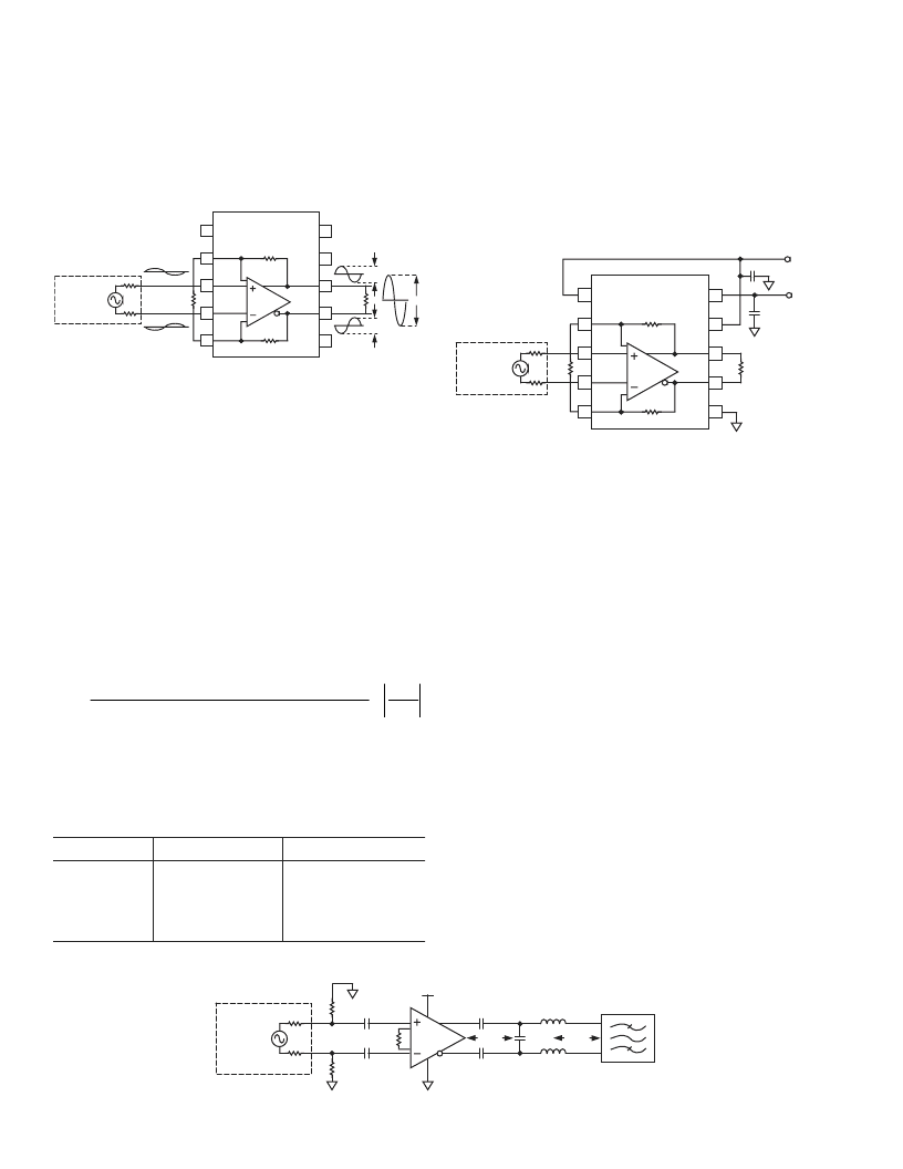
BASIC CONCEPTS
Differential signaling is used in high performance signal chains,
where distortion performance, signal-to-noise ratio, and low power
consumption is critical. Differential circuits inherently provide
improved common-mode rejection and harmonic distortion perfor-
mance as well as better immunity to interference and ground noise.
VOCM
10
VPOS
9
OPHI
8
OPLO
7
COMM
6
1
PWUP
RGP1
2
INHI
3
INLO
4
RGP2
5
R
G
BALANCED
SOURCE
R
L
A
A
2A
Figure 1. Differential Circuit Representation
Figure 1 illustrates the expected input and output waveforms for
a typical application. Usually the applied input waveform will be
a balanced differential drive, where the signal applied to the INHI
and INLO pins are equal in amplitude and differ in phase by 180
°
.
In some applications, baluns may be used to transform a single-
ended drive signal to a differential signal. The AD8351 may also be
used to transform a single-ended signal to a differential signal.
GAIN ADJUSTMENT
The differential gain of the AD8351 is set using a single external
resistor, R
G
, which is connected between Pins 2 and 5. The gain
can be set to any value between 0 dB and 26 dB using the resistor
values specified in TPC 2, with common gain values provided in
Table I. The board traces used to connect the external gain resis-
tor should be balanced and as short as possible to help prevent
noise pickup and to ensure balanced gain and stability. The low
frequency voltage gain of the AD8351 can be modeled as
A
R
4 6 19 5
.
R
R
R
R
R
R
R
R
R
V
V
V
L
G
F
+
L
G
L
G
L
F
G
OUT
IN
=
×
(
.
)
+
×
×
×
×
×
+
(
)
×
+
(
)
=
5 6
.
9.
39
where:
R
F
is 350
(internal).
R
L
is the single-ended load resistance.
R
G
is the gain setting resistor.
Table I. Gain Resistor Selection for Common Gain Values
(Load Resistance Is Specified as Single-Ended)
Gain, A
V
R
G
(R
L
= 75 )
0 dB
680
6 dB
200
10 dB
100
20 dB
22
R
G
(R
L
= 500 )
2 k
470
200
43
COMMON-MODE ADJUSTMENT
The output common-mode voltage level is the dc offset voltage
present at each of the differential outputs. The ac signals are of
equal amplitude with a 180
°
phase difference but are centered
at the same common-mode voltage level. The common-mode
output voltage level can be adjusted from 1.2 V to 3.8 V by
driving the desired voltage level into the VOCM pin, as illus-
trated in Figure 2.
VOCM
10
VPOS
9
OPHI
8
OPLO
7
COMM
6
1
PWUP
RGP1
2
INHI
3
INLO
4
RGP2
5
R
G
BALANCED
SOURCE
R
L
0.1 F
V
S
V
OCM
1.2V
TO
3.8V
C
DECL
0.1 F
Figure 2. Common-Mode Adjustment
INPUT AND OUTPUT MATCHING
The AD8351 provides a moderately high differential input
impedance of 5 k
. In practical applications, the input of the
AD8351 will be terminated to a lower impedance to provide an
impedance match to the driving source, as depicted in Figure 3.
The terminating resistor, R
T
, should be as close as possible to
the input pins in order to minimize reflections due to imped-
ance mismatch. The 150
output impedance may need to be
transformed to provide the desired output match to a given
load. Matching components can be calculated using a Smith
Chart or by using a resonant approach to determine the match-
ing network that results in a complex conjugate match. The
input and output impedances and reflection coefficients are
provided in TPCs 19, 20, 22, and 23. For additional informa-
tion on reactive matching to differential sources and loads, refer
to the Applications section of the AD8350 data sheet.
Figure 3 illustrates a SAW (surface acoustic wave) filter inter-
face. Many SAW filters are inherently differential, allowing for a
low loss output match. In this example, the SAW filter requires
a 50
source impedance in order to provide the desired center
frequency and Q. The series L shunt C output network provides
a 150
to 50
impedance transformation at the desired frequency
of operation. The impedance transformation is illustrated on a Smith
Chart in Figure 4.
It is possible to drive a single-ended SAW filter simply by con-
necting the unused output to ground using the appropriate
terminating resistance. The overall gain of the system will be
reduced by 6 dB due to the fact that only half of the signal will
be available to the input of the SAW filter.
BALANCED
SOURCE
R
S
R
S
R
S
= R
T
R
T
R
T
0.1 F
0.1 FR
G
0.1 F
0.1 F
150
C
P
8pF
L
S
27nF
L
S
27nF
50
190MHz SAW
VPOS
AD8351
Figure 3. Example of Differential SAW Filter Interface (f
C
= 190 MHz)
相關PDF資料 |
PDF描述 |
|---|---|
| AD8354 | 100 MHz-2.7 GHz RF Gain Block |
| AD8354ACP-R2 | 100 MHz-2.7 GHz RF Gain Block |
| AD8354-EVAL | 100 MHz-2.7 GHz RF Gain Block |
| AD8354ACP-REEL7 | 100 MHz-2.7 GHz RF Gain Block |
| AD835 | 250 MHz, Voltage Output 4-Quadrant Multiplier |
相關代理商/技術參數 |
參數描述 |
|---|---|
| AD8351ARMZ | 功能描述:IC DIFF AMP RF/IF LOWDIST 10MSOP RoHS:是 類別:RF/IF 和 RFID >> RF 放大器 系列:- 標準包裝:3,000 系列:- 頻率:100MHz ~ 6GHz P1dB:9.14dBm(8.2mW) 增益:15.7dB 噪音數據:1.3dB RF 型:CDMA,TDMA,PCS 電源電壓:2.7 V ~ 5 V 電流 - 電源:60mA 測試頻率:2GHz 封裝/外殼:0505(1412 公制) 包裝:帶卷 (TR) |
| AD8351ARMZ-REEL7 | 功能描述:IC DIFF AMP RF/IF LD 10MSOP RoHS:是 類別:RF/IF 和 RFID >> RF 放大器 系列:- 標準包裝:3,000 系列:- 頻率:100MHz ~ 6GHz P1dB:9.14dBm(8.2mW) 增益:15.7dB 噪音數據:1.3dB RF 型:CDMA,TDMA,PCS 電源電壓:2.7 V ~ 5 V 電流 - 電源:60mA 測試頻率:2GHz 封裝/外殼:0505(1412 公制) 包裝:帶卷 (TR) |
| AD8351-EVAL | 制造商:Analog Devices 功能描述:MINISO IF SAMPLING ADC DRIVER - Bulk |
| AD8351-EVALZ | 制造商:Analog Devices 功能描述:LOW DISTORTION DIFFERENTIAL RF/IF AMP - Bulk |
| AD8351SCPZ-EP-R7 | 功能描述:EP LFCSP PACKAGE 制造商:analog devices inc. 系列:- 包裝:帶卷(TR) 零件狀態:在售 頻率:2.2GHz P1dB:- 增益:1dB 噪聲系數:- RF 類型:- 電壓 - 電源:3 V ~ 5.5 V 電流 - 電源:28mA 測試頻率:2.2GHz 封裝/外殼:16-WFQFN 裸露焊盤 供應商器件封裝:16-LFCSP(3x3) 標準包裝:1,500 |
發布緊急采購,3分鐘左右您將得到回復。