- 您現在的位置:買賣IC網 > PDF目錄373945 > AD8362ARU (ANALOG DEVICES INC) 50 Hz to 2.7 GHz 60 dB TruPwr⑩ Detector PDF資料下載
參數資料
| 型號: | AD8362ARU |
| 廠商: | ANALOG DEVICES INC |
| 元件分類: | 模擬信號調理 |
| 英文描述: | 50 Hz to 2.7 GHz 60 dB TruPwr⑩ Detector |
| 中文描述: | SPECIALTY ANALOG CIRCUIT, PDSO16 |
| 封裝: | MO-153AB, TSSOP-16 |
| 文件頁數: | 30/36頁 |
| 文件大小: | 700K |
| 代理商: | AD8362ARU |
第1頁第2頁第3頁第4頁第5頁第6頁第7頁第8頁第9頁第10頁第11頁第12頁第13頁第14頁第15頁第16頁第17頁第18頁第19頁第20頁第21頁第22頁第23頁第24頁第25頁第26頁第27頁第28頁第29頁當前第30頁第31頁第32頁第33頁第34頁第35頁第36頁
AD8362
If optimized for use at lower frequencies, CFLT should be
increased accordingly; for audio applications, use 0.1 μF. In RF
measurements where the carrier frequency is known, the
coupling and bandwidth limiting between the ICs might be
provided by a narrow-band SAW filter. Figure 62 shows the
output and law conformance error for this AD8330/AD8362
collaboration. The dynamic range extends from 5 μV to 0.5 V
rms between the 0.5 dB error points in this simulation.
Rev. B | Page 30 of 36
RMS INPUT VOLTAGE (V)
E
4
3
2
1
–1
–3
5
μ
500
μ
5m
50m
500m
50
μ
O
0
0
–2
3
2
1
0
Figure 62. Output and Conformance for the AD8330/AD8362 Collaboration
RF POWER METER WITH 80 DB RANGE
According to simulations, the basic 60 dB measurement range
of the AD8362 can be extended by up to 20 dB by using a target
voltage, VTGT, that increases progressively with the input level.
In the simplest case, this can be achieved by connecting VTGT
to the output VOUT/VSET. Figure 63 shows the connections;
for present purposes, R1 is omitted and R2 is short-circuited.
For small signal inputs, VOUT is also small, and the target is
well below the normal 75 mV (with 1.25 V applied to VTGT).
The lower target means that the AD8362’s VGA output does
not have to be as large as normal, which increases the input
sensitivity. As the signal and thus VOUT increases, so does the
target voltage, which progressively shifts the required VGA
input to a higher level.
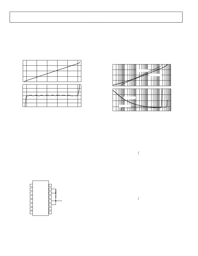
16
15
14
13
12
11
10
9
1
2
3
4
5
6
7
8
COMM
CHPF
DECL
INHI
INLO
DECL
PWDN
COMM
ACOM
VREF
VTGT
VPOS
VOUT
VSET
ACOM
CLPF
AD8362
V
OUT
R2
R1
0
Figure 63. RF Power Meter with 80 dB Range
For example, a 10:1 change of VTGT from 0.35 V to 3.5 V shifts
the intercept by 20 dB. This has the effect of stretching the
measurement range by the same amount, from >60 dB to more
than 80 dB. So the slope decreases to about 40 mV/dB because a
larger input range is now represented by the same 3.15 V. The
simulation results shown in Figure 64 compare the expanded
range response with that for a fixed VTGT. The upper end of
the measurement range is extended from 1.5 V to over 4 V
(limited by the input protection).
RMS INPUT VOLTAGE (V)
D
100
μ
1m
10m
10
O
0
5
10
15
0
1
3
4
0.1
1
2
V
TGT
= V
OUT
V
TGT
= 1.25V
V
TGT
= V
OUT
V
TGT
= 1.25V
0
Figure 64. Dynamic Range Expansion Using VTGT = VOUT
However, it is apparent that the transfer function is no
longer a simple logarithmic law; further consideration shows
that the modified function is nonanalytic. Nevertheless, this
function is dependable, and it remains as stable over supply
and temperature variations as in the normal mode. A good
approximation is provided by
(
10
log
IN
P
SL
V
V
V
VOUT
′
)
(
)
[
]
{
}
3
10
log
m
3
11
IN
Z
V
=
(16)
where the modified slope voltage
V
SLP
'
'
is 0.868 V, that is,
43.4 mV/dB. Using this expression, the dynamic range is 86 dB
to the ±0.5 dB error points (0.2 mV ≤ V
IN
≤ 4 V). The actual
range is reduced in practice by the effects of the AD8362’s
input-referred noise at low inputs. If the basic 60 dB+ range is
only slightly less than required in a particular application, then
a fraction of VOUT can be summed with a part of VREF to the
VTGT pin, which is why R1 and R2 were included. The output
now conforms in general terms to the formula
(
10
log
IN
P
SL
V
V
V
VOUT
′
)
(
)
[
]
{
}
3
10
log
IN
C
Z
V
K
=
′
(17)
where the correction factor
K
C
introduces the required
nonlinear correction to minimize the law-conformance error.
Table 5 provides several representative spot values using
progressively greater amounts of dynamic range extension.
相關PDF資料 |
PDF描述 |
|---|---|
| AD8362ARU-REEL7 | 50 Hz to 2.7 GHz 60 dB TruPwr⑩ Detector |
| AD8362ARUZ-REEL71 | 50 Hz to 2.7 GHz 60 dB TruPwr⑩ Detector |
| AD8362ARUZ1 | 50 Hz to 2.7 GHz 60 dB TruPwr⑩ Detector |
| AD8367ARU-REEL | 500 MHz, Linear-in-dB VGA with AGC Detector |
| AD8367-EVAL | RECTIFIER STANDARD SINGLE 1A 50V 50 30A-ifsm 5uA-ir 1V-vf DO-41 5K/REEL-13 |
相關代理商/技術參數 |
參數描述 |
|---|---|
| AD8362ARU-REEL | 制造商:AD 制造商全稱:Analog Devices 功能描述:50 Hz to 3.8 GHz 65 dB TruPwr? Detector |
| AD8362ARU-REEL7 | 功能描述:IC PWR DETECTOR 3.8GHZ 16-TSSOP RoHS:否 類別:RF/IF 和 RFID >> RF 檢測器 系列:- 產品變化通告:Product Discontinuation 15/May/2006 標準包裝:3,000 系列:- 頻率:100MHz ~ 2GHz RF 型:手機,GSM,DCS,PCS 輸入范圍:- 精確度:- 電源電壓:2.7 V ~ 5.5 V 電流 - 電源:300µA 包裝:帶卷 (TR) 封裝/外殼:SC-74,SOT-457 其它名稱:NCS5000SNT1GOS |
| AD8362ARUZ | 功能描述:IC PWR DETECTOR 3.8GHZ 16-TSSOP RoHS:是 類別:RF/IF 和 RFID >> RF 檢測器 系列:- 產品變化通告:Product Discontinuation 15/May/2006 標準包裝:3,000 系列:- 頻率:100MHz ~ 2GHz RF 型:手機,GSM,DCS,PCS 輸入范圍:- 精確度:- 電源電壓:2.7 V ~ 5.5 V 電流 - 電源:300µA 包裝:帶卷 (TR) 封裝/外殼:SC-74,SOT-457 其它名稱:NCS5000SNT1GOS |
| AD8362ARUZ | 制造商:Analog Devices 功能描述:RMS Detector IC |
| AD8362ARUZ1 | 制造商:AD 制造商全稱:Analog Devices 功能描述:50 Hz to 2.7 GHz 60 dB TruPwr⑩ Detector |
發布緊急采購,3分鐘左右您將得到回復。