- 您現(xiàn)在的位置:買賣IC網(wǎng) > PDF目錄373945 > AD8362ARUZ-REEL71 (Analog Devices, Inc.) 50 Hz to 2.7 GHz 60 dB TruPwr⑩ Detector PDF資料下載
參數(shù)資料
| 型號: | AD8362ARUZ-REEL71 |
| 廠商: | Analog Devices, Inc. |
| 英文描述: | 50 Hz to 2.7 GHz 60 dB TruPwr⑩ Detector |
| 中文描述: | 50赫茲到2.7 GHz 60分貝TruPwr⑩探測器 |
| 文件頁數(shù): | 25/36頁 |
| 文件大小: | 700K |
| 代理商: | AD8362ARUZ-REEL71 |
第1頁第2頁第3頁第4頁第5頁第6頁第7頁第8頁第9頁第10頁第11頁第12頁第13頁第14頁第15頁第16頁第17頁第18頁第19頁第20頁第21頁第22頁第23頁第24頁當(dāng)前第25頁第26頁第27頁第28頁第29頁第30頁第31頁第32頁第33頁第34頁第35頁第36頁
AD8362
lowers the signal currents in the squaring cells by a factor of 25.
As well as making the system more sensitive to small static
errors (offsets) in the postdetection circuitry, such a reduction
also reduces the peak slew rate. A suitable adjustment to the
value of CLPF is needed to maintain a given AGC loop
bandwidth. On the other hand, increasing the target voltage can
improve the accuracy and stability of the intercept for low crest
factor signals. Thus, using VTGT = 2.5 V, the peak output
currents of the squaring cell are quadrupled and the peak slew
rate is increased by the same factor. CLPF should be increased
to maintain an adequate stability margin in the AGC loop.
Rev. B | Page 25 of 36
In many applications, it is useful to use a nonstandard value of
VTGT to shift the measurement range by a constant amount to
accommodate either a reduced or increased range of signal
inputs. The dynamic span remains >60 dB for such changes.
This technique is particularly useful when the sensitivity can be
lowered by raising VTGT, and there is little expectation of high
crest factor signals.
ADJUSTING THE INTERCEPT
Another way to take advantage of the effect of
VTGT
is to use it
to introduce an adjustment to the log intercept, represented by
the voltage
V
Z
in Equation 14. Formally, this can be expressed in
terms of a modified value of
V
Z
'
.
V
VTGT
V
V
Z
Z
'
25
.
=
(14)
A lower
VTGT
effectively increases the sensitivity of the
measurement system, which is just another way of stating that the
intercept moves to a lower value. This raises VOUT for all input
amplitudes, as demonstrated by the plots in Figure 45. This
control of the measurement system’s intercept could therefore be
brought about by applying the output of a DAC to the VTGT pin,
if that suits the overall objectives of an application.
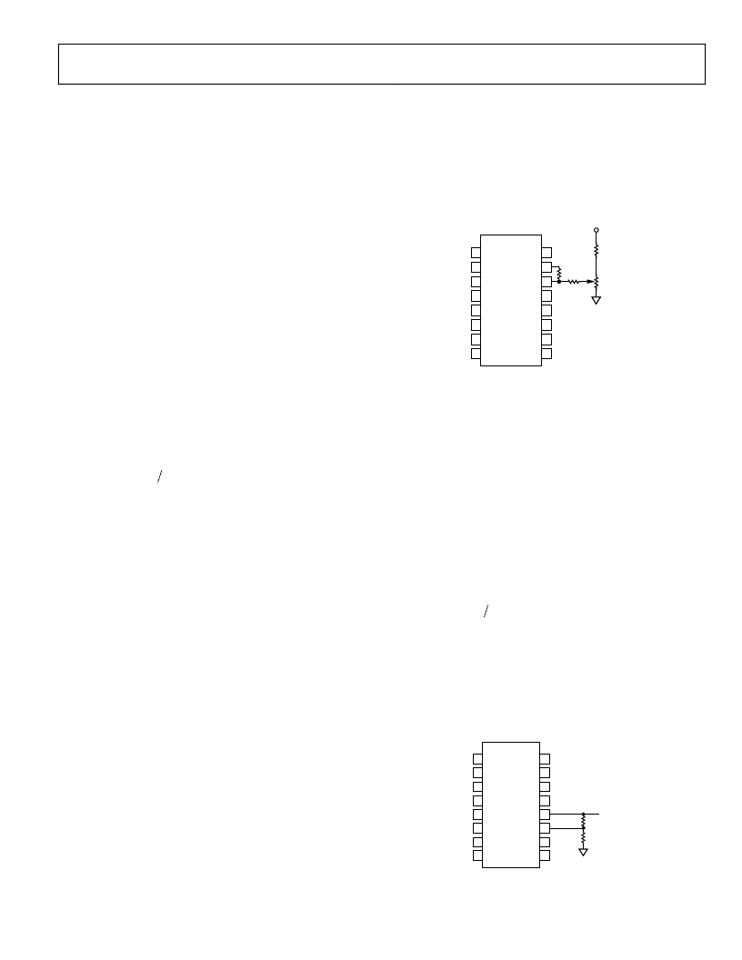
For many purposes, a small manual adjustment range of ±3 dB
is sufficient. This can be implemented as shown in Figure 55.
Here, the largest fraction of VTGT is still provided by the built-
in reference to minimize the sensitivity to supply voltage
variations. Now a variable component is provided by the trim
network. For a 5 V supply, this added component of VTGT is 0
when VR1 is centered. With the slider closest to ground, VTGT
is lowered by 366 mV, which corresponds to a 3 dB decrease in
intercept; in the opposite condition, it is raised by 518 mV,
which increases the intercept by 3 dB. That is, VTGT ranges
from 1.25 V/√2 to √2 × 1.25 V.
Other adjustment ranges can be readily calculated from this
example. The resistance at the VTGT pin is nominally 52 k;
resistor values should be calculated with this in mind. In some
situations, this control interface might be driven from a
programmable source. In the simplest case, a logic level could
provide two intercept values, differing by say, 10 dB, thus
providing essentially two switched input ranges.
Also, it is worth remembering that these shifts in intercept are
equivalent, in most respects, to a dc offset applied to the
AD8362’s output, with the main differences being that:
Varying VTGT affects the crest factor capacity to some
extent
This technique makes better use of the available output
range than a post-VOUT adjustment would
16
15
14
13
12
11
10
9
1
2
3
4
5
6
7
8
COMM
CHPF
DECL
INHI
INLO
DECL
PWDN
COMM
ACOM
VREF
VTGT
VPOS
VOUT
VSET
ACOM
CLPF
AD8362
5V
4.02k
4.02k
5.75k
VR1
20k
0
Figure 55. Adjustments of the Intercept by ±3 dB
ALTERING THE SLOPE
None of the changes in operating conditions discussed so far
affect the logarithmic slope, V
SLP
, in Equation 9. However, this
can readily be altered by controlling the fraction of VOUT that
is fed back to the setpoint interface at the VSET pin. When the
full signal from VOUT is applied to VSET, the slope assumes its
nominal value of 50 mV/dB. It can be increased by including an
attenuator between these pins, as shown in Figure 56. Moder-
ately low resistance values should be used to minimize scaling
errors due to the 70 k input resistance at the VSET pin. Keep
in mind that this resistor string also loads the output, and it
eventually reduces the load-driving capabilities if very low
values are used. To calculate the resistor values, use
(
50
=
D
R2
R1
)
1
'
S
(15)
where
S
D
is the desired slope, expressed in mV/dB, and
R2'
is the value of R2 in parallel with 70 k. For example, using
R1 = 1.65 k and R2 = 1.69 k (R2' = 1.649 k), the nominal
slope is increased to 100 mV/dB. This choice of scaling is useful
when the output is applied to a digital voltmeter because the
displayed number reads as a decibel quantity directly, with only
a decimal point shift.
16
15
14
13
12
11
10
9
1
2
3
4
5
6
7
8
COMM
CHPF
DECL
INHI
INLO
DECL
PWDN
COMM
ACOM
VREF
VTGT
VPOS
VOUT
VSET
ACOM
CLPF
AD8362
V
OUT
R1
R2
0
Figure 56. External Network to Raise Slope
相關(guān)PDF資料 |
PDF描述 |
|---|---|
| AD8362ARUZ1 | 50 Hz to 2.7 GHz 60 dB TruPwr⑩ Detector |
| AD8367ARU-REEL | 500 MHz, Linear-in-dB VGA with AGC Detector |
| AD8367-EVAL | RECTIFIER STANDARD SINGLE 1A 50V 50 30A-ifsm 5uA-ir 1V-vf DO-41 5K/REEL-13 |
| AD8367ARU-REEL-7 | 500 MHz, Linear-in-dB VGA with AGC Detector |
| AD8367 | 500 MHz, Linear-in-dB VGA with AGC Detector |
相關(guān)代理商/技術(shù)參數(shù) |
參數(shù)描述 |
|---|---|
| AD8362-EVAL | 制造商:Analog Devices 功能描述:RF DETECTOR, 50 HZ TO 2.7GHZ 60 DB TRUPWR DETECTOR - Bulk |
| AD8362-EVALZ | 功能描述:BOARD EVAL FOR AD8362 RoHS:是 類別:RF/IF 和 RFID >> RF 評估和開發(fā)套件,板 系列:TruePower™ 標(biāo)準(zhǔn)包裝:1 系列:- 類型:GPS 接收器 頻率:1575MHz 適用于相關(guān)產(chǎn)品:- 已供物品:模塊 其它名稱:SER3796 |
| AD8363 | 制造商:AD 制造商全稱:Analog Devices 功能描述:50 Hz to 6 GHz, 50 dB TruPwr? Detector |
| AD8363_09 | 制造商:AD 制造商全稱:Analog Devices 功能描述:50 Hz to 6 GHz, 50 dB TruPwr? Detector |
| AD8363ACPZ-R2 | 制造商:Analog Devices 功能描述:TRUE RMS PWR DETECTOR 24LFCSP EP - Tape and Reel |
發(fā)布緊急采購,3分鐘左右您將得到回復(fù)。