- 您現在的位置:買賣IC網 > PDF目錄373959 > AD9211_07 (Analog Devices, Inc.) 10-Bit, 200 MSPS/250 MSPS/300 MSPS, 1.8 V Analog-to-Digital Converter PDF資料下載
參數資料
| 型號: | AD9211_07 |
| 廠商: | Analog Devices, Inc. |
| 英文描述: | 10-Bit, 200 MSPS/250 MSPS/300 MSPS, 1.8 V Analog-to-Digital Converter |
| 中文描述: | 10位,200 MSPS/250 MSPS/300 MSPS的,1.8 V模擬到數字轉換器 |
| 文件頁數: | 20/28頁 |
| 文件大小: | 1180K |
| 代理商: | AD9211_07 |
第1頁第2頁第3頁第4頁第5頁第6頁第7頁第8頁第9頁第10頁第11頁第12頁第13頁第14頁第15頁第16頁第17頁第18頁第19頁當前第20頁第21頁第22頁第23頁第24頁第25頁第26頁第27頁第28頁
AD9211
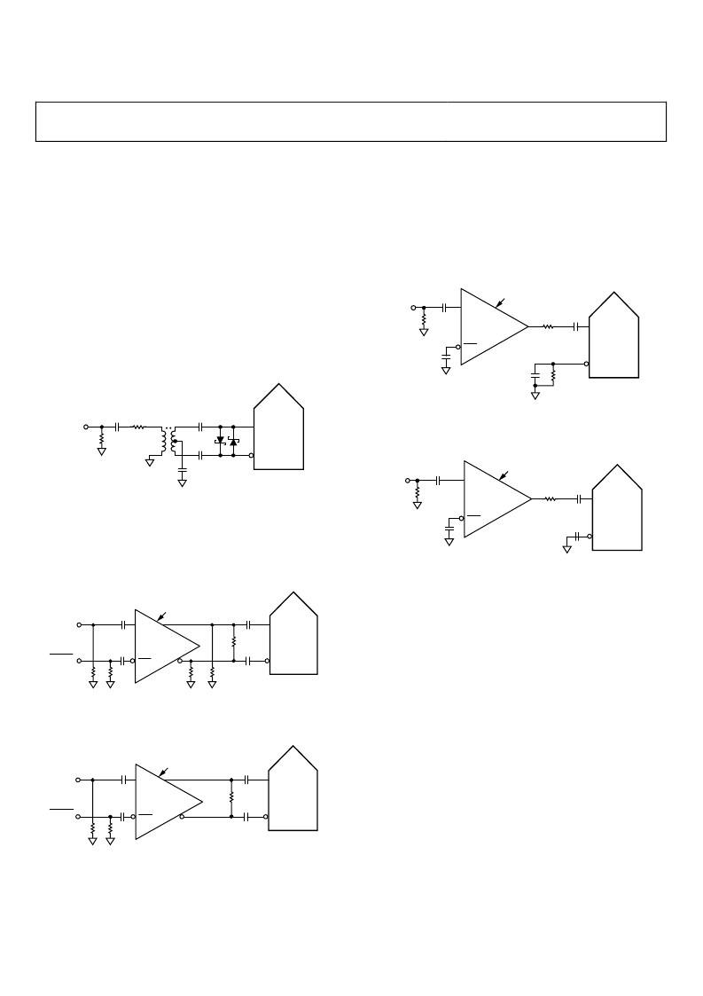
CLOCK INPUT CONSIDERATIONS
For optimum performance, the AD9211 sample clock inputs
(CLK+ and CLK) should be clocked with a differential signal.
This signal is typically ac-coupled into the CLK+ pin and CLK
pin via a transformer or capacitors. These pins are biased
internally and require no additional bias.
Figure 42 shows one preferred method for clocking the AD9211.
The low jitter clock source is converted from single-ended to
differential using an RF transformer. The back-to-back Schottky
diodes across the secondary transformer limit clock excursions
into the AD9211 to approximately 0.8 V p-p differential. This
helps prevent the large voltage swings of the clock from feeding
through to other portions of the AD9211 and preserves the fast
rise and fall times of the signal, which are critical to low jitter
performance.
Rev. 0 | Page 20 of 28
0.1μF
0.1μF
0.1μF
0.1μF
CLOCK
INPUT
50
100
CLK–
CLK+
ADC
AD9211
MINI-CIRCUITS
ADT1–1WT, 1:1Z
XFMR
SCHOTTKY
DIODES:
HSM2812
0
Figure 42. Transformer-Coupled Differential Clock
If a low jitter clock is available, another option is to ac couple a
differential PECL signal to the sample clock input pins, as
shown in Figure 43. The
AD9510
/
AD9511
/
AD9512
/
AD9513
/
AD9514
/
AD9515
family of clock drivers offers excellent jitter
performance.
100
0.1μF
0.1μF
0.1μF
0.1μF
240
240
AD9510/AD9511/
AD9512/AD9513/
AD9514/AD9515
50
*
50
*
CLK
CLK
*
50
RESISTORS ARE OPTIONAL.
CLK–
CLK+
ADC
AD9211
PECL DRIVER
INPUT
CLOCK
INPUT
0
Figure 43. Differential PECL Sample Clock
CLOCK
INPUT
CLOCK
INPUT
100
0.1μF
0.1μF
0.1μF
0.1μF
50
*
LVDS DRIVER
50
*
CLK
CLK
*50
RESISTORS ARE OPTIONAL.
CLK–
CLK+
ADC
AD9211
AD9510/AD9511/
AD9512/AD9513/
AD9514/AD9515
0
Figure 44. Differential LVDS Sample Clock
In some applications, it is acceptable to drive the sample clock
inputs with a single-ended CMOS signal. In such applications,
CLK+ should be directly driven from a CMOS gate, and the
CLK pin should be bypassed to ground with a 0.1 μF capacitor
in parallel with a 39 kΩ resistor (see Figure 45). Although the
CLK+ input circuit supply is AVDD (1.8 V), this input is
designed to withstand input voltages up to 3.3 V, making the
selection of the drive logic voltage very flexible.
0.1μF
0.1μF
0.1μF
39k
CMOS DRIVER
50
*
OPTIONAL
100
0.1μF
CLK
CLK
*50
RESISTOR IS OPTIONAL.
Figure 45. Single-Ended 1.8 V CMOS Sample Clock
CLK–
CLK+
ADC
AD9211
AD9510/AD9511/
AD9512/AD9513/
AD9514/AD9515
CLOCK
INPUT
0
0.1μF
0.1μF
0.1μF
CMOS DRIVER
CLK
CLK
*
50
RESISTOR IS OPTIONAL.
0.1μF
CLK–
CLK+
AD9510/AD9511/
AD9512/AD9513/
AD9514/AD9515
ADC
AD9211
CLOCK
INPUT
50
*
OPTIONAL
100
0
Figure 46. Single-Ended 3.3 V CMOS Sample Clock
Clock Duty Cycle Considerations
Typical high speed ADCs use both clock edges to generate a
variety of internal timing signals. As a result, these ADCs may
be sensitive to clock duty cycle. Commonly, a 5% tolerance is
required on the clock duty cycle to maintain dynamic performance
characteristics. The AD9211 contains a duty cycle stabilizer (DCS)
that retimes the nonsampling edge, providing an internal clock
signal with a nominal 50% duty cycle. This allows a wide range
of clock input duty cycles without affecting the performance of
the AD9211. When the DCS is on, noise and distortion perfor-
mance are nearly flat for a wide range of duty cycles. However,
some applications may require the DCS function to be off. If so,
keep in mind that the dynamic range performance can be affected
when operated in this mode. See the AD9211 Configuration
Using the SPI section for more details on using this feature.
The duty cycle stabilizer uses a delay-locked loop (DLL) to
create the nonsampling edge. As a result, any changes to the
sampling frequency require approximately eight clock cycles
to allow the DLL to acquire and lock to the new rate.
相關PDF資料 |
PDF描述 |
|---|---|
| AD9211-200EBZ | 10-Bit, 200 MSPS/250 MSPS/300 MSPS, 1.8 V Analog-to-Digital Converter |
| AD9211-250EBZ | 10-Bit, 200 MSPS/250 MSPS/300 MSPS, 1.8 V Analog-to-Digital Converter |
| AD9211-300EBZ | 10-Bit, 200 MSPS/250 MSPS/300 MSPS, 1.8 V Analog-to-Digital Converter |
| AD9211BCPZ-300 | 10-Bit, 200 MSPS/250 MSPS/300 MSPS, 1.8 V Analog-to-Digital Converter |
| AD9211 | 10-Bit, 170/200/250 MSPS 1.8 V A/D Converter |
相關代理商/技術參數 |
參數描述 |
|---|---|
| AD9211-170EB | 制造商:AD 制造商全稱:Analog Devices 功能描述:10-Bit, 170/200/250 MSPS 1.8 V A/D Converter |
| AD9211-200EB | 制造商:AD 制造商全稱:Analog Devices 功能描述:10-Bit, 170/200/250 MSPS 1.8 V A/D Converter |
| AD9211-200EBZ | 功能描述:BOARD EVAL FOR AD9211-200 RoHS:是 類別:編程器,開發系統 >> 評估板 - 模數轉換器 (ADC) 系列:- 產品培訓模塊:Obsolescence Mitigation Program 標準包裝:1 系列:- ADC 的數量:1 位數:12 采樣率(每秒):94.4k 數據接口:USB 輸入范圍:±VREF/2 在以下條件下的電源(標準):- 工作溫度:-40°C ~ 85°C 已用 IC / 零件:MAX11645 已供物品:板,軟件 |
| AD9211-250EB | 制造商:AD 制造商全稱:Analog Devices 功能描述:10-Bit, 170/200/250 MSPS 1.8 V A/D Converter |
| AD9211-250EBZ | 功能描述:數據轉換 IC 開發工具 10-Bit 250 Msps ADC RoHS:否 制造商:Texas Instruments 產品:Demonstration Kits 類型:ADC 工具用于評估:ADS130E08 接口類型:SPI 工作電源電壓:- 6 V to + 6 V |
發布緊急采購,3分鐘左右您將得到回復。