- 您現在的位置:買賣IC網 > PDF目錄373959 > AD9211_07 (Analog Devices, Inc.) 10-Bit, 200 MSPS/250 MSPS/300 MSPS, 1.8 V Analog-to-Digital Converter PDF資料下載
參數資料
| 型號: | AD9211_07 |
| 廠商: | Analog Devices, Inc. |
| 英文描述: | 10-Bit, 200 MSPS/250 MSPS/300 MSPS, 1.8 V Analog-to-Digital Converter |
| 中文描述: | 10位,200 MSPS/250 MSPS/300 MSPS的,1.8 V模擬到數字轉換器 |
| 文件頁數: | 23/28頁 |
| 文件大小: | 1180K |
| 代理商: | AD9211_07 |
第1頁第2頁第3頁第4頁第5頁第6頁第7頁第8頁第9頁第10頁第11頁第12頁第13頁第14頁第15頁第16頁第17頁第18頁第19頁第20頁第21頁第22頁當前第23頁第24頁第25頁第26頁第27頁第28頁
AD9211
Table 9. Serial Port Pins
Mnemonic
SCLK
Rev. 0 | Page 23 of 28
HARDWARE INTERFACE
The pins described in Table 9 comprise the physical interface
between the user’s programming device and the serial port of
the AD9211. All serial pins are inputs with an open-drain
configuration and should be tied to an external pull-up or pull-
down resistor (suggested value of 10 kΩ).
This interface is flexible enough to be controlled by either
PROMS or PIC mirocontrollers as well. This provides the user
with an alternate method to program the ADC other than a SPI
controller.
If the user chooses not to use the SPI interface, some pins serve
a dual function and are associated with a specific function when
strapped externally to AVDD or ground during device power
on. The Configuration Without the SPI section describes the
strappable functions supported on the AD9230.
CONFIGURATION WITHOUT THE SPI
In applications that do not interface to the SPI control registers,
the SPI SDIO/DCS and SPI SCLK/DFS pins can alternately
serve as standalone CMOS-compatible control pins. When the
device is powered up, it is assumed that the user intends to use
the pins as static control lines for the duty cycle stabilizer. In
this mode, the SPI CSB chip select should be connected to
ground, which disables the serial port interface.
Function
SCLK (Serial Clock) is the serial shift clock in.
SCLK is used to synchronize serial interface
reads and writes.
SDIO (Serial Data Input/Output) is a dual-purpose
pin. The typical role for this pin is an input and
output depending on the instruction being sent
and the relative position in the timing frame.
CSB (Chip Select Bar) is an active low control that
gates the read and write cycles.
Master Device Reset. When asserted, device
assumes default settings. Active low.
SDIO
CSB
RESET
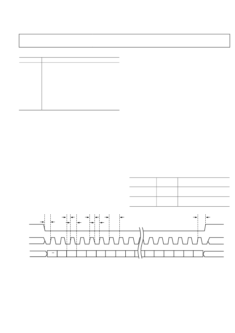
The falling edge of the CSB, in conjunction with the rising edge
of the SCLK, determines the start of the framing. An example of
the serial timing and its definitions can be found in Figure 51
and Table 11.
During an instruction phase, a 16-bit instruction is transmitted.
Data then follows the instruction phase and is determined by
the W0 and W1 bits, which is 1 or more bytes of data. All data is
composed of 8-bit words. The first bit of each individual byte of
serial data indicates whether this is a read or write command.
This allows the serial data input/output (SDIO) pin to change
direction from an input to an output.
Data may be sent in MSB or in LSB first mode. MSB first is
default on power-up and can be changed by changing the con-
figuration register. For more information about this feature and
others, see the
AN-877
,
Interfacing to High Speed ADCs via SPI
.
Table 10. Mode Selection
Mnemonic
SPI SDIO/DCS
External
Voltage
AVDD
AGND
AVDD
AGND
Configuration
Duty cycle stabilizer enabled
Duty cycle stabilizer disabled
Twos complement enabled
Offset binary enabled
SPI SCLK/DFS
DON’T CARE
DON’T CARE
DON’T CARE
DON’T CARE
SDIO
SCLK
CSB
t
S
t
DH
t
HI
t
CLK
t
LO
t
DS
t
H
R/W
W1
W0
A12
A11
A10
A9
A8
A7
D5
D4
D3
D2
D1
D0
0
Figure 51. Serial Port Interface Timing Diagram
相關PDF資料 |
PDF描述 |
|---|---|
| AD9211-200EBZ | 10-Bit, 200 MSPS/250 MSPS/300 MSPS, 1.8 V Analog-to-Digital Converter |
| AD9211-250EBZ | 10-Bit, 200 MSPS/250 MSPS/300 MSPS, 1.8 V Analog-to-Digital Converter |
| AD9211-300EBZ | 10-Bit, 200 MSPS/250 MSPS/300 MSPS, 1.8 V Analog-to-Digital Converter |
| AD9211BCPZ-300 | 10-Bit, 200 MSPS/250 MSPS/300 MSPS, 1.8 V Analog-to-Digital Converter |
| AD9211 | 10-Bit, 170/200/250 MSPS 1.8 V A/D Converter |
相關代理商/技術參數 |
參數描述 |
|---|---|
| AD9211-170EB | 制造商:AD 制造商全稱:Analog Devices 功能描述:10-Bit, 170/200/250 MSPS 1.8 V A/D Converter |
| AD9211-200EB | 制造商:AD 制造商全稱:Analog Devices 功能描述:10-Bit, 170/200/250 MSPS 1.8 V A/D Converter |
| AD9211-200EBZ | 功能描述:BOARD EVAL FOR AD9211-200 RoHS:是 類別:編程器,開發系統 >> 評估板 - 模數轉換器 (ADC) 系列:- 產品培訓模塊:Obsolescence Mitigation Program 標準包裝:1 系列:- ADC 的數量:1 位數:12 采樣率(每秒):94.4k 數據接口:USB 輸入范圍:±VREF/2 在以下條件下的電源(標準):- 工作溫度:-40°C ~ 85°C 已用 IC / 零件:MAX11645 已供物品:板,軟件 |
| AD9211-250EB | 制造商:AD 制造商全稱:Analog Devices 功能描述:10-Bit, 170/200/250 MSPS 1.8 V A/D Converter |
| AD9211-250EBZ | 功能描述:數據轉換 IC 開發工具 10-Bit 250 Msps ADC RoHS:否 制造商:Texas Instruments 產品:Demonstration Kits 類型:ADC 工具用于評估:ADS130E08 接口類型:SPI 工作電源電壓:- 6 V to + 6 V |
發布緊急采購,3分鐘左右您將得到回復。