- 您現在的位置:買賣IC網 > PDF目錄373959 > AD9211BCPZ-250 (ANALOG DEVICES INC) 10-Bit, 170/200/250 MSPS 1.8 V A/D Converter PDF資料下載
參數資料
| 型號: | AD9211BCPZ-250 |
| 廠商: | ANALOG DEVICES INC |
| 元件分類: | ADC |
| 英文描述: | 10-Bit, 170/200/250 MSPS 1.8 V A/D Converter |
| 中文描述: | 1-CH 10-BIT PROPRIETARY METHOD ADC, PARALLEL ACCESS, QCC56 |
| 封裝: | 8 X 8 MM, ROHS COMPLIANT, MO-220VLLD-2, LFCSP-56 |
| 文件頁數: | 19/21頁 |
| 文件大小: | 310K |
| 代理商: | AD9211BCPZ-250 |
Preliminary Technical Data
AD9211
HARDWARE INTERFACE
The pins described in Table X comprise the physical interface
between the user’s programming device and the serial port of
the AD9211. All serial pins are inputs, which is an open-drain
output and should be tied to an external pull-up or pull-down
resistor (suggested value 10 kΩ).
Rev. PrA | Page 19 of 21
This interface is flexible enough to be controlled by either
PROMS or PIC mirocontrollers as well. This provides the user
to use an alternate method to program the ADC other than a
SPI controller.
If the user chooses to not use the SPI interface, some pins serve
a dual function and are associated with a specific function when
strapped externally to AVDD or ground during device power
on. The section below describes the strappable functions
supported on the AD9211. AD9211
CONFIGURATION WITHOUT THE SPI
In applications that do not interface to the SPI control registers,
the SPI SDIO / DCS and SPI SCLK / DFS pins can alternately
serve as stand alone CMOS compatible control pins When the
device is powered up, it is assumed that the user intends to use
the pins as static control lines for the duty cycle stabilizer. In
this mode the SPI CSB chip select should be connected to
AVDD, which will disable the serial port interface.
Table 6. Mode Selection
Pin
External
Voltage
AVDD
SPI SDIO / DCS
AGND
AVDD
SPI SCLK / DFS
AGND
READING THE MEMORY MAP TABLE
Each row in the memory map table has eight address locations.
The memory map is roughly divided into four sections: chip
Configuration
Duty Cycle Stabilizer Enabled
Duty Cycle Stabilizer Disabled
2’s Complement Enabled
Offset Binary Enabled
configuration register map (Address 0x00 to Address 0x02),
device index and transfer register map (Address 0x04 to
Address 0x05, and Address 0xFF), global ADC function register
map (Address 0x08 to Address 0x09), and flexible ADC
functions register map (Address 0x0B to Address 0x25). The
flexible ADC functions register map is product specific.
Starting from the right hand column, the memory map register
in Table X documents the default hex value for each hex address
shown. The column with the heading Byte 7 (MSB) is the start
of the default hex value giving. For example, hex address 0x14,
flex_output_phase has a hex default value of 00h. This means
Bit 3 = 0, Bit 2 = 0, Bit 1 = 1, and Bit 0 = 1 or 0011 in binary.
This setting is the default output clock or DCO phase adjust
option. The default value adjusts the DCO phase 90deg relative
to the Nominal DCO edge and 180deg relative to the data edge.
For more information on this function and others consult the
SPI Doc at www.analog.com.
OPEN LOCATIONS
All locations marked as “open” are currently not supported for
this particular device. When required, these locations should be
written with 0s. Writing to these locations is required only when
part of an address location is open (for example, Address 0x14).
If the whole address location is open (for example, Address
0x13), then this address location does not need to be written.
DEFAULT VALUES
Coming out of reset, some of the address locations (but not all)
are loaded with default values. The default values for the
registers are given in the Table X.
LOGIC LEVELS
An explanation of various registers, “bit is set” is synonymous
with “bit is set to Logic 1” or “writing Logic 1 for the bit.”
Similarly “clear a bit” is synonymous with “bit is set to Logic 0”
or “writing Logic 0 for the bit.”
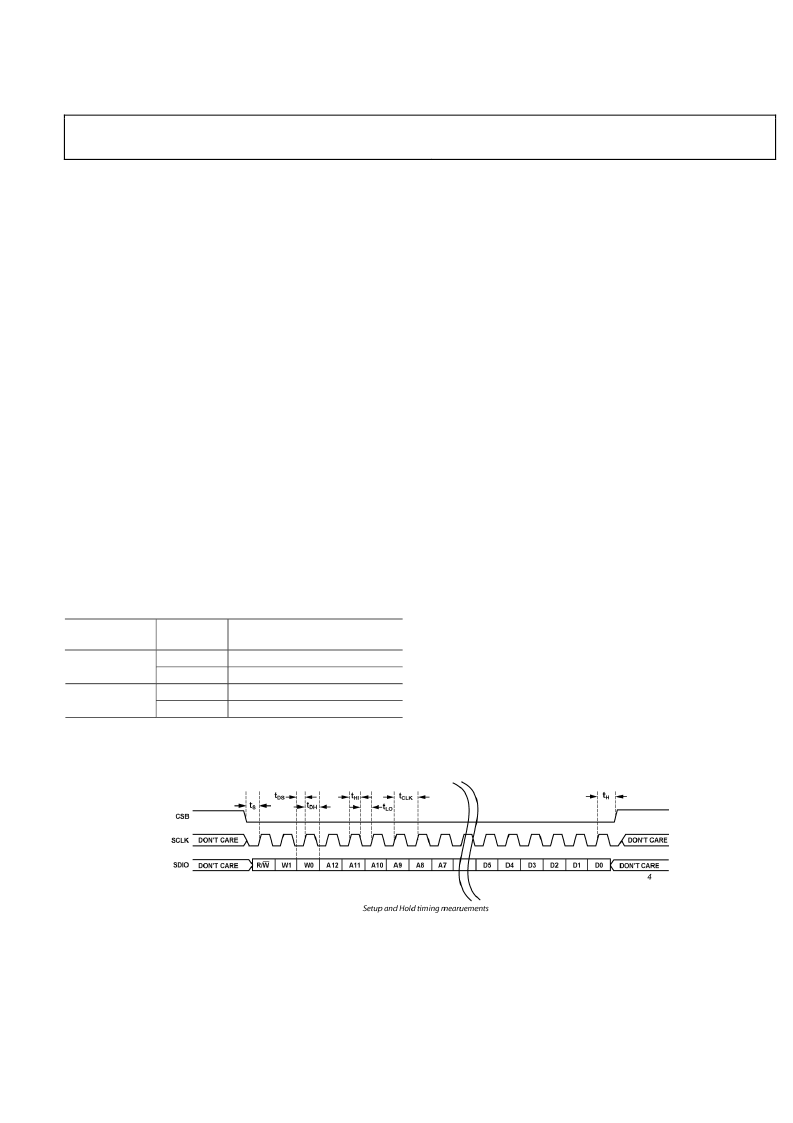
Figure X. Serial Port Interface Timing Diagram
相關PDF資料 |
PDF描述 |
|---|---|
| AD9212 | Octal, 10-Bit, 40/65 MSPS Serial LVDS 1.8 V A/D Converter |
| AD9212-65EBZ | Octal, 10-Bit, 40/65 MSPS Serial LVDS 1.8 V A/D Converter |
| AD9212BCPZ-40 | Octal, 10-Bit, 40/65 MSPS Serial LVDS 1.8 V A/D Converter |
| AD9212BCPZ-65 | Octal, 10-Bit, 40/65 MSPS Serial LVDS 1.8 V A/D Converter |
| AD9212BCPZRL7-40 | Octal, 10-Bit, 40/65 MSPS Serial LVDS 1.8 V A/D Converter |
相關代理商/技術參數 |
參數描述 |
|---|---|
| AD9211BCPZ-300 | 功能描述:IC ADC 10BIT 300MSPS 56LFCSP RoHS:是 類別:集成電路 (IC) >> 數據采集 - 模數轉換器 系列:- 其它有關文件:TSA1204 View All Specifications 標準包裝:1 系列:- 位數:12 采樣率(每秒):20M 數據接口:并聯 轉換器數目:2 功率耗散(最大):155mW 電壓電源:模擬和數字 工作溫度:-40°C ~ 85°C 安裝類型:表面貼裝 封裝/外殼:48-TQFP 供應商設備封裝:48-TQFP(7x7) 包裝:Digi-Reel® 輸入數目和類型:4 個單端,單極;2 個差分,單極 產品目錄頁面:1156 (CN2011-ZH PDF) 其它名稱:497-5435-6 |
| AD9212 | 制造商:AD 制造商全稱:Analog Devices 功能描述:Octal, 10-Bit, 40/65 MSPS Serial LVDS 1.8 V A/D Converter |
| AD9212_11 | 制造商:AD 制造商全稱:Analog Devices 功能描述:Octal, 10-Bit, 40 MSPS/65 MSPS, Serial LVDS, 1.8 V ADC |
| AD9212-65EB1 | 制造商:AD 制造商全稱:Analog Devices 功能描述:High Speed ADC USB FIFO Evaluation Kit |
| AD9212-65EBZ | 功能描述:BOARD EVALUATION FOR AD9212 RoHS:是 類別:編程器,開發系統 >> 評估板 - 模數轉換器 (ADC) 系列:- 產品培訓模塊:Obsolescence Mitigation Program 標準包裝:1 系列:- ADC 的數量:1 位數:12 采樣率(每秒):94.4k 數據接口:USB 輸入范圍:±VREF/2 在以下條件下的電源(標準):- 工作溫度:-40°C ~ 85°C 已用 IC / 零件:MAX11645 已供物品:板,軟件 |
發布緊急采購,3分鐘左右您將得到回復。