- 您現在的位置:買賣IC網 > PDF目錄373960 > AD9224 (Analog Devices, Inc.) Complete 12-Bit 40 MSPS Monolithic A/D Converter PDF資料下載
參數資料
| 型號: | AD9224 |
| 廠商: | Analog Devices, Inc. |
| 英文描述: | Complete 12-Bit 40 MSPS Monolithic A/D Converter |
| 中文描述: | 完整的12位40 MSPS的單片A / D轉換 |
| 文件頁數: | 17/24頁 |
| 文件大小: | 309K |
| 代理商: | AD9224 |
AD9224
–17–
REV. A
Resistor Programmable Reference
Figure 28 shows an example of how to generate a reference
voltage other than 1.0 V or 2.0 V with the addition of two exter-
nal resistors and a bypass capacitor. Use the equation,
VREF
= 1
V
×
(1 +
R
1/
R
2),
to determine appropriate values for R1 and R2. These resistors
should be in the 2 k
to 100 k
range. For the example shown,
R1 equals 2.5 k
and R2 equals 5 k
. From the equation
above, the resultant reference voltage on the VREF pin is 1.5 V.
This sets the input span to be 3 V p-p. To assure stability, place
a 0.1
μ
F ceramic capacitor in parallel with R1.
1.5V
C1
0.1
m
F
10
m
F
VINA
VINB
VREF
SENSE
REFCOM
AD9224
4V
1V
2.5V
R1
2.5k
V
R2
5k
V
0.1
m
F
Figure 28. Resistor Programmable Reference—3 V p-p
Input Span, V
CM
= 2.5 V
The midscale voltage can be set to VREF by connecting VINB
to VREF to provide an input span of 0 to 2
×
VREF. Alterna-
tively, the midscale voltage can be set to 2.5 V by connecting
VINB to a low impedance 2.5 V source. For the example shown,
the valid input single-ended range for VINA is 1 V to 4 V since
VINB is set to an external, low impedance 2.5 V source. The
VREF pin should be bypassed to the REFCOM pin with a
10
μ
F tantalum capacitor in parallel with a low inductance
0.1
μ
F ceramic capacitor.
USING AN EXTERNAL REFERENCE
Using an external reference may enhance the dc performance
of the AD9224 by improving drift and accuracy. Figures 29 and
30 show examples of how to use an external reference with the
A/D. Table III is a list of suitable voltage references from Ana-
log Devices. To use an external reference, the user must disable
the internal reference amplifier and drive the VREF pin.
Connecting the SENSE pin to AVDD disables the internal
reference amplifier.
Table III. Suitable Voltage References
Initial
Accuracy
% (max)
Output
Voltage
Drift
(ppm/
8
C)
Operating
Current
Internal
AD589
AD1580
REF191
Internal
1.00
1.235
1.225
2.048
2.0
26
10–100
50–100
5–25
26
1.4
1.2–2.8
0.08–0.8
0.1–0.5
1.4
1 mA
50
μ
A
50
μ
A
45
μ
A
1 mA
The AD9224 contains an internal reference buffer, A2 (see
Figure 16), that simplifies the drive requirements of an external
reference. The external reference must be able to drive about
5 k
(
±
20%) load. Note that the bandwidth of the reference
buffer is deliberately left small to minimize the reference noise
contribution. As a result, it is not possible to change the refer-
ence voltage rapidly in this mode.
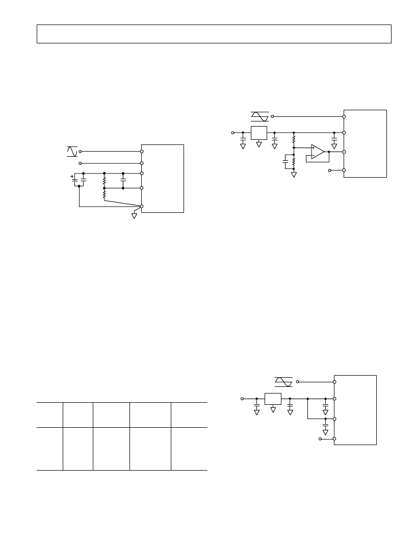
2.5V+VREF
2.5V–VREF
2.5V
+5V
0.1
m
F
22
m
F
VINA
VINB
VREF
SENSE
AD9224
+5V
R2
0.1
m
F
A1
R1
0.1
m
F
2.5V
REF
Figure 29. External Reference
Variable Input Span with V
CM
= 2.5 V
Figure 29 shows an example of the AD9224 configured for an
input span of 2
×
VREF centered at 2.5 V. An external 2.5 V
reference drives the VINB pin thus setting the common-mode
voltage at 2.5 V. The input span can be independently set by a
voltage divider consisting of R1 and R2 which generates the
VREF signal. A1 buffers this resistor network and drives
VREF. Choose this op amp based on accuracy requirements. It
is essential that a minimum of a 10
μ
F capacitor in parallel with
a 0.1
μ
F low inductance ceramic capacitor decouple the A1’s
output to ground.
Single-Ended Input with 0 to 2
3
VREF Range
Figure 30 shows an example of an external reference driving
both VINB and VREF. In this case, both the common-mode
voltage and input span are directly dependent on the value of
VREF. More specifically, the common-mode voltage is equal to
VREF while the input span is equal to 2
×
VREF. Thus, the
valid input range extends from 0 to 2
×
VREF. For example, if
the REF191, a 2.048 V external reference was selected, the
valid input range extends from 0 to 4.096 V. In this case, 1 LSB
of the AD9224 corresponds to 1 mV. It is essential that a mini-
mum of a 10
μ
F capacitor in parallel with a 0.1
μ
F low inductance
ceramic capacitor decouple the reference output to ground.
2
3
REF
0V
+5V
10
m
F
VINA
VINB
VREF
SENSE
AD9224
+5V
0.1
m
F
VREF
0.1
m
F
0.1
m
F
Figure 30. Input Range = 0 V to 2
×
VREF
相關PDF資料 |
PDF描述 |
|---|---|
| AD9224-EB | Complete 12-Bit 40 MSPS Monolithic A/D Converter |
| AD9225 | Complete 12-Bit, 25 MSPS Monolithic A/D Converter |
| AD9225-EB | Complete 12-Bit, 25 MSPS Monolithic A/D Converter |
| AD9225AR | Complete 12-Bit, 25 MSPS Monolithic A/D Converter |
| AD9225ARS | Complete 12-Bit, 25 MSPS Monolithic A/D Converter |
相關代理商/技術參數 |
參數描述 |
|---|---|
| AD9224ARS | 制造商:Analog Devices 功能描述:Analog/Digital Converter IC Number of Bi |
| AD9224ARSZ | 功能描述:IC ADC 12BIT 40MSPS 28-SSOP RoHS:是 類別:集成電路 (IC) >> 數據采集 - 模數轉換器 系列:- 標準包裝:1 系列:microPOWER™ 位數:8 采樣率(每秒):1M 數據接口:串行,SPI? 轉換器數目:1 功率耗散(最大):- 電壓電源:模擬和數字 工作溫度:-40°C ~ 125°C 安裝類型:表面貼裝 封裝/外殼:24-VFQFN 裸露焊盤 供應商設備封裝:24-VQFN 裸露焊盤(4x4) 包裝:Digi-Reel® 輸入數目和類型:8 個單端,單極 產品目錄頁面:892 (CN2011-ZH PDF) 其它名稱:296-25851-6 |
| AD9224ARSZRL | 功能描述:IC ADC 12BIT 40MSPS 28SSOP RoHS:是 類別:集成電路 (IC) >> 數據采集 - 模數轉換器 系列:- 標準包裝:1,000 系列:- 位數:12 采樣率(每秒):300k 數據接口:并聯 轉換器數目:1 功率耗散(最大):75mW 電壓電源:單電源 工作溫度:0°C ~ 70°C 安裝類型:表面貼裝 封裝/外殼:24-SOIC(0.295",7.50mm 寬) 供應商設備封裝:24-SOIC 包裝:帶卷 (TR) 輸入數目和類型:1 個單端,單極;1 個單端,雙極 |
| AD9224-EB | 制造商:Analog Devices 功能描述:Evaluation Kit For Complete 12-Bit, 40 MSPS Monolithic A/D Converter 制造商:Analog Devices 功能描述:EVAL KIT FOR COMPLETE 12-BIT, 40 MSPS MONOLITHIC A/D CNVRTR - Bulk 制造商:Rochester Electronics LLC 功能描述:12-BIT 40 MSPS MONOLITHIC A/D CONVERTER - Bulk |
| AD9224JR | 制造商:未知廠家 制造商全稱:未知廠家 功能描述:Analog-to-Digital Converter, 12-Bit |
發布緊急采購,3分鐘左右您將得到回復。