- 您現在的位置:買賣IC網 > PDF目錄373960 > AD9224 (Analog Devices, Inc.) Complete 12-Bit 40 MSPS Monolithic A/D Converter PDF資料下載
參數資料
| 型號: | AD9224 |
| 廠商: | Analog Devices, Inc. |
| 英文描述: | Complete 12-Bit 40 MSPS Monolithic A/D Converter |
| 中文描述: | 完整的12位40 MSPS的單片A / D轉換 |
| 文件頁數: | 21/24頁 |
| 文件大小: | 309K |
| 代理商: | AD9224 |
AD9224
–21–
REV. A
GROUNDING AND DECOUPLING
Analog and Digital Grounding
Proper grounding is essential in any high speed, high resolution
system. Multilayer printed circuit boards (PCBs) are recom-
mended to provide optimal grounding and power schemes. The
use of ground and power planes offers distinct advantages:
1. The minimization of the loop area encompassed by a signal
and its return path.
2. The minimization of the impedance associated with ground
and power paths.
3. The inherent distributed capacitor formed by the power
plane, PCB insulation and ground plane.
These characteristics result in both a reduction of electromag-
netic interference (EMI) and an overall improvement in
performance.
It is important to design a layout that prevents noise from cou-
pling onto the input signal. Digital signals should not be run in
parallel with input signal traces and should be routed away from
the input circuitry. While the AD9224 features separate analog
and driver ground pins, it should be treated as an analog com-
ponent. The AVSS and DRVSS pins must be joined together
directly under the AD9224. A solid ground plane under the A/D
is acceptable if the power and ground return currents are care-
fully managed. Alternatively, the ground plane under the A/D
may contain serrations to steer currents in predictable directions
where cross coupling between analog and digital would other-
wise be unavoidable. The AD9224/AD9225EB ground layout,
shown in Figure 47, depicts the serrated type of arrangement.
The evaluation board is primarily built over a common ground
plane. It has a “slit” to route currents near the clock driver. Figure
40 illustrates a general scheme of ground and power implementa-
tion in and around the AD9224.
ANALOG
CIRCUITS
DIGITAL
LOGIC
ICs
D
V
A
A
D
DVSS
AVSS
A
B
I
A
I
D
AVDD
DVDD
LOGIC
SUPPLY
D
A
V
IN
C
STRAY
C
STRAY
GND
A
= ANALOG
D
= DIGITAL
ADC
IC
DIGITAL
CIRCUITS
A
A
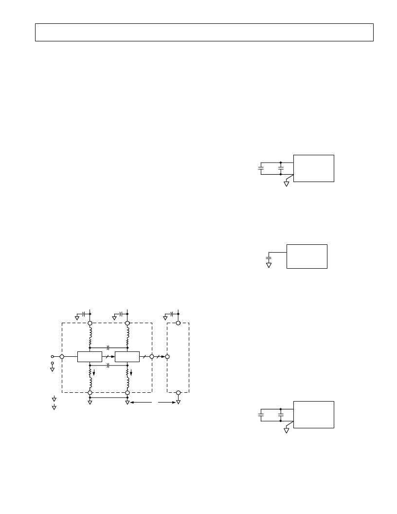
Figure 40. Ground and Power Consideration
Analog and Digital Driver Supply Decoupling
The AD9224 features separate analog and digital supply and
ground pins, helping to minimize digital corruption of sensitive
analog signals. In general, AVDD, the analog supply, should be
decoupled to AVSS, the analog common, as close to the chip as
physically possible. Figure 41 shows the recommended decou-
pling for the analog supplies; 0.1
μ
F ceramic chip and 10
μ
F
tantalum capacitors should provide adequately low impedance
over a wide frequency range. Note that the AVDD and AVSS
pins are colocated on the AD9224 to simplify the layout of the
decoupling capacitors and provide the shortest possible PCB
trace lengths. The AD9224/AD9225EB power plane layout,
shown in Figure 48 depicts a typical arrangement using a multi-
layer PCB.
0.1
m
F
AVDD
AVSS
AD9224
10
m
F
Figure 41. Analog Supply Decoupling
The CML is an internal analog bias point used internally by the
AD9224. This pin must be decoupled with at least a 0.1
μ
F
capacitor as shown in Figure 42. The dc level of CML is ap-
proximately AVDD/2. This voltage should be buffered if it is to
be used for any external biasing.
0.1
m
F
CML
AD9224
Figure 42. CML Decoupling
The digital activity on the AD9224 chip falls into two general
categories: correction logic, and output drivers. The internal
correction logic draws relatively small surges of current, mainly
during the clock transitions. The output drivers draw large
current impulses while the output bits are changing. The size
and duration of these currents are a function of the load on the
output bits: large capacitive loads are to be avoided. Note, the
internal correction logic of the AD9224 is referenced to AVDD
while the output drivers are referenced to DRVDD.
The decoupling shown in Figure 43, a 0.1
μ
F ceramic chip and
10
μ
F tantalum capacitors are appropriate for a reasonable
capacitive load on the digital outputs (typically 20 pF on each
pin). Applications involving greater digital loads should consider
increasing the digital decoupling proportionally, and/or using
external buffers/latches.
0.1
m
F
DRVDD
DRVSS
AD9224
10
m
F
Figure 43. Digital Supply Decoupling
A complete decoupling scheme will also include large tantalum
or electrolytic capacitors on the PCB to reduce low frequency
ripple to negligible levels. Refer to the AD9224/AD9225EB
schematic and layouts in Figures 44-50 for more information
regarding the placement of decoupling capacitors.
相關PDF資料 |
PDF描述 |
|---|---|
| AD9224-EB | Complete 12-Bit 40 MSPS Monolithic A/D Converter |
| AD9225 | Complete 12-Bit, 25 MSPS Monolithic A/D Converter |
| AD9225-EB | Complete 12-Bit, 25 MSPS Monolithic A/D Converter |
| AD9225AR | Complete 12-Bit, 25 MSPS Monolithic A/D Converter |
| AD9225ARS | Complete 12-Bit, 25 MSPS Monolithic A/D Converter |
相關代理商/技術參數 |
參數描述 |
|---|---|
| AD9224ARS | 制造商:Analog Devices 功能描述:Analog/Digital Converter IC Number of Bi |
| AD9224ARSZ | 功能描述:IC ADC 12BIT 40MSPS 28-SSOP RoHS:是 類別:集成電路 (IC) >> 數據采集 - 模數轉換器 系列:- 標準包裝:1 系列:microPOWER™ 位數:8 采樣率(每秒):1M 數據接口:串行,SPI? 轉換器數目:1 功率耗散(最大):- 電壓電源:模擬和數字 工作溫度:-40°C ~ 125°C 安裝類型:表面貼裝 封裝/外殼:24-VFQFN 裸露焊盤 供應商設備封裝:24-VQFN 裸露焊盤(4x4) 包裝:Digi-Reel® 輸入數目和類型:8 個單端,單極 產品目錄頁面:892 (CN2011-ZH PDF) 其它名稱:296-25851-6 |
| AD9224ARSZRL | 功能描述:IC ADC 12BIT 40MSPS 28SSOP RoHS:是 類別:集成電路 (IC) >> 數據采集 - 模數轉換器 系列:- 標準包裝:1,000 系列:- 位數:12 采樣率(每秒):300k 數據接口:并聯 轉換器數目:1 功率耗散(最大):75mW 電壓電源:單電源 工作溫度:0°C ~ 70°C 安裝類型:表面貼裝 封裝/外殼:24-SOIC(0.295",7.50mm 寬) 供應商設備封裝:24-SOIC 包裝:帶卷 (TR) 輸入數目和類型:1 個單端,單極;1 個單端,雙極 |
| AD9224-EB | 制造商:Analog Devices 功能描述:Evaluation Kit For Complete 12-Bit, 40 MSPS Monolithic A/D Converter 制造商:Analog Devices 功能描述:EVAL KIT FOR COMPLETE 12-BIT, 40 MSPS MONOLITHIC A/D CNVRTR - Bulk 制造商:Rochester Electronics LLC 功能描述:12-BIT 40 MSPS MONOLITHIC A/D CONVERTER - Bulk |
| AD9224JR | 制造商:未知廠家 制造商全稱:未知廠家 功能描述:Analog-to-Digital Converter, 12-Bit |
發(fā)布緊急采購,3分鐘左右您將得到回復。