- 您現在的位置:買賣IC網 > PDF目錄373961 > AD9228-65EB (Analog Devices, Inc.) Quad, 12-bit, 40/65 MSPS Serial LVDS 1.8 V A/D Converter PDF資料下載
參數資料
| 型號: | AD9228-65EB |
| 廠商: | Analog Devices, Inc. |
| 英文描述: | Quad, 12-bit, 40/65 MSPS Serial LVDS 1.8 V A/D Converter |
| 中文描述: | 四,12位,六十五分之四十○MSPS的串行LVDS 1.8弗吉尼亞州/ D轉換器 |
| 文件頁數: | 19/52頁 |
| 文件大小: | 1659K |
| 代理商: | AD9228-65EB |
第1頁第2頁第3頁第4頁第5頁第6頁第7頁第8頁第9頁第10頁第11頁第12頁第13頁第14頁第15頁第16頁第17頁第18頁當前第19頁第20頁第21頁第22頁第23頁第24頁第25頁第26頁第27頁第28頁第29頁第30頁第31頁第32頁第33頁第34頁第35頁第36頁第37頁第38頁第39頁第40頁第41頁第42頁第43頁第44頁第45頁第46頁第47頁第48頁第49頁第50頁第51頁第52頁
AD9228
THEORY OF OPERATION
The AD9228 architecture consists of a pipelined ADC that is
divided into three sections: a 4-bit first stage followed by eight
1.5-bit stages and a final 3-bit flash. Each stage provides
sufficient overlap to correct for flash errors in the preceding
stages. The quantized outputs from each stage are combined
into a final 12-bit result in the digital correction logic. The
pipelined architecture permits the first stage to operate on a
new input sample while the remaining stages operate on preceding
samples. Sampling occurs on the rising edge of the clock.
Rev. 0 | Page 19 of 52
Each stage of the pipeline, excluding the last, consists of a low
resolution flash ADC connected to a switched-capacitor DAC
and interstage residue amplifier (MDAC). The residue amplifier
magnifies the difference between the reconstructed DAC output
and the flash input for the next stage in the pipeline. One bit of
redundancy is used in each stage to facilitate digital correction
of flash errors. The last stage simply consists of a flash ADC.
The output staging block aligns the data, carries out the error
correction, and passes the data to the output buffers. The data is
then serialized and aligned to the frame and output clock.
ANALOG INPUT CONSIDERATIONS
The analog input to the AD9228 is a differential switched-capacitor
circuit designed for processing differential input signals. The input
can support a wide common-mode range and maintain excellent
performance. An input common-mode voltage of midsupply
minimizes signal-dependent errors and provides optimum
performance.
S
S
H
C
PAR
C
SAMPLE
C
SAMPLE
C
PAR
VIN–
H
S
S
H
VIN+
H
0
Figure 43. Switched-Capacitor Input Circuit
The clock signal alternately switches the input circuit between
sample mode and hold mode (see Figure 43). When the input
circuit is switched into sample mode, the signal source must be
capable of charging the sample capacitors and settling within
one-half of a clock cycle. A small resistor in series with each
input can help reduce the peak transient current injected from
the output stage of the driving source. In addition, low-Q inductors
or ferrite beads can be placed on each leg of the input to reduce
the high differential capacitance seen at the analog inputs, thus
realizing the maximum bandwidth of the ADC. Such use of
low-Q inductors or ferrite beads is required when driving the
converter front end at high IF frequencies. Either a shunt capacitor
or two single-ended capacitors can be placed on the inputs to
provide a matching passive network. This ultimately creates a
low-pass filter at the input to limit any unwanted broadband
noise. See the
AN-742 Application Note
, the
AN-827 Application
Note
, and the
Analog Dialogue
article “
Transformer-Coupled
Front-End for Wideband A/D Converters
” for more information
on this subject. In general, the precise values depend on the
application.
The analog inputs of the AD9228 are not internally dc-biased.
In ac-coupled applications, the user must provide this bias
externally. Setting the device so that
V
CM
=
AVDD
/2 is recom-
mended for optimum performance, but the device can function
over a wider range with reasonable performance, as shown in
Figure 44 and Figure 45.
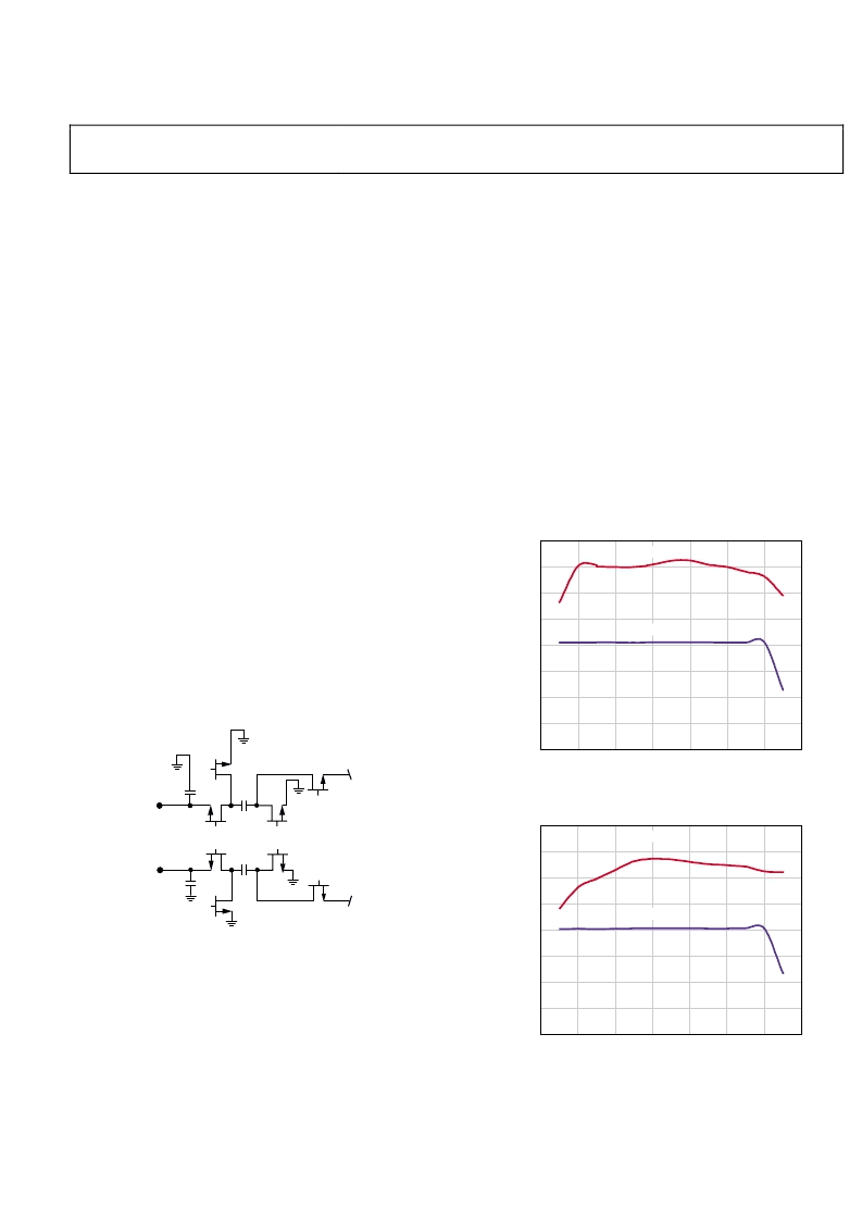
S
ANALOG INPUT COMMON MODE VOLTAGE (V)
0
50
55
60
65
70
75
80
85
90
0.2
0.4
0.6
0.8
1.0
1.2
1.4
1.6
SFDR (dBc)
SNR (dB)
Figure 44. SNR/SFDR vs. Common-Mode Voltage,
f
IN
= 2.4 MHz, f
SAMPLE
= 65 MSPS
S
ANALOG INPUT COMMON MODE VOLTAGE (V)
0
50
55
60
65
70
75
80
85
90
0.2
0.4
0.6
0.8
1.0
1.2
1.4
1.6
SFDR (dBc)
SNR (dB)
Figure 45. SNR/SFDR vs. Common-Mode Voltage,
f
IN
= 30 MHz, f
SAMPLE
= 65 MSPS
相關PDF資料 |
PDF描述 |
|---|---|
| AD9229BCP-50 | Quad 12-Bit, 50/65 MSPS Serial LVDS 3V A/D Converter |
| AD9229BCP-65 | Quad 12-Bit, 50/65 MSPS Serial LVDS 3V A/D Converter |
| AD9229 | Quad 12-Bit, 50/65 MSPS Serial LVDS 3V A/D Converter |
| AD9235 | 12-Bit, 20/40/65 MSPS 3 V A/D Converter |
| AD9235BCP-20 | 12-Bit, 20/40/65 MSPS 3 V A/D Converter |
相關代理商/技術參數 |
參數描述 |
|---|---|
| AD9228-65EB1 | 制造商:AD 制造商全稱:Analog Devices 功能描述:High Speed ADC USB FIFO Evaluation Kit |
| AD9228-65EBZ | 功能描述:BOARD EVAL FOR AD9228 RoHS:是 類別:編程器,開發系統 >> 評估板 - 模數轉換器 (ADC) 系列:- 產品培訓模塊:Obsolescence Mitigation Program 標準包裝:1 系列:- ADC 的數量:1 位數:12 采樣率(每秒):94.4k 數據接口:USB 輸入范圍:±VREF/2 在以下條件下的電源(標準):- 工作溫度:-40°C ~ 85°C 已用 IC / 零件:MAX11645 已供物品:板,軟件 |
| AD9228ABCPZ-40 | 功能描述:IC ADC 12BIT SPI/SRL 40M 48LFCSP RoHS:是 類別:集成電路 (IC) >> 數據采集 - 模數轉換器 系列:- 其它有關文件:TSA1204 View All Specifications 標準包裝:1 系列:- 位數:12 采樣率(每秒):20M 數據接口:并聯 轉換器數目:2 功率耗散(最大):155mW 電壓電源:模擬和數字 工作溫度:-40°C ~ 85°C 安裝類型:表面貼裝 封裝/外殼:48-TQFP 供應商設備封裝:48-TQFP(7x7) 包裝:Digi-Reel® 輸入數目和類型:4 個單端,單極;2 個差分,單極 產品目錄頁面:1156 (CN2011-ZH PDF) 其它名稱:497-5435-6 |
| AD9228ABCPZ-65 | 功能描述:IC ADC 12BIT SPI/SRL 65M 48LFCSP RoHS:是 類別:集成電路 (IC) >> 數據采集 - 模數轉換器 系列:- 其它有關文件:TSA1204 View All Specifications 標準包裝:1 系列:- 位數:12 采樣率(每秒):20M 數據接口:并聯 轉換器數目:2 功率耗散(最大):155mW 電壓電源:模擬和數字 工作溫度:-40°C ~ 85°C 安裝類型:表面貼裝 封裝/外殼:48-TQFP 供應商設備封裝:48-TQFP(7x7) 包裝:Digi-Reel® 輸入數目和類型:4 個單端,單極;2 個差分,單極 產品目錄頁面:1156 (CN2011-ZH PDF) 其它名稱:497-5435-6 |
| AD9228ABCPZRL7-40 | 功能描述:IC ADC 12BIT SPI/SRL 40M 48LFCSP RoHS:是 類別:集成電路 (IC) >> 數據采集 - 模數轉換器 系列:- 標準包裝:1 系列:- 位數:14 采樣率(每秒):83k 數據接口:串行,并聯 轉換器數目:1 功率耗散(最大):95mW 電壓電源:雙 ± 工作溫度:0°C ~ 70°C 安裝類型:通孔 封裝/外殼:28-DIP(0.600",15.24mm) 供應商設備封裝:28-PDIP 包裝:管件 輸入數目和類型:1 個單端,雙極 |
發布緊急采購,3分鐘左右您將得到回復。