- 您現在的位置:買賣IC網 > PDF目錄373961 > AD9228 (Analog Devices, Inc.) Quad, 12-bit, 40/65 MSPS Serial LVDS 1.8 V A/D Converter PDF資料下載
參數資料
| 型號: | AD9228 |
| 廠商: | Analog Devices, Inc. |
| 英文描述: | Quad, 12-bit, 40/65 MSPS Serial LVDS 1.8 V A/D Converter |
| 中文描述: | 四,12位,六十五分之四十○MSPS的串行LVDS 1.8弗吉尼亞州/ D轉換器 |
| 文件頁數: | 20/52頁 |
| 文件大小: | 1659K |
| 代理商: | AD9228 |
第1頁第2頁第3頁第4頁第5頁第6頁第7頁第8頁第9頁第10頁第11頁第12頁第13頁第14頁第15頁第16頁第17頁第18頁第19頁當前第20頁第21頁第22頁第23頁第24頁第25頁第26頁第27頁第28頁第29頁第30頁第31頁第32頁第33頁第34頁第35頁第36頁第37頁第38頁第39頁第40頁第41頁第42頁第43頁第44頁第45頁第46頁第47頁第48頁第49頁第50頁第51頁第52頁
AD9228
For best dynamic performance, the source impedances driving
VIN+ and VIN should be matched such that common-mode
settling errors are symmetrical. These errors are reduced by the
common-mode rejection of the ADC. An internal reference
buffer creates the positive and negative reference voltages, REFT
and REFB, respectively, that define the span of the ADC core.
The output common-mode of the reference buffer is set to
midsupply, and the REFT and REFB voltages and span are
defined as
REFT
= 1/2 (
AVDD
+
VREF
)
REFB
= 1/2 (
AVDD
VREF
)
Span
= 2 × (
REFT
REFB
) = 2 ×
VREF
Rev. 0 | Page 20 of 52
It can be seen from these equations that the REFT and REFB
voltages are symmetrical about the midsupply voltage and, by
definition, the input span is twice the value of the VREF voltage.
Maximum SNR performance is always achieved by setting the
ADC to the largest span in a differential configuration. In the
case of the AD9228, the largest input span available is 2 V p-p.
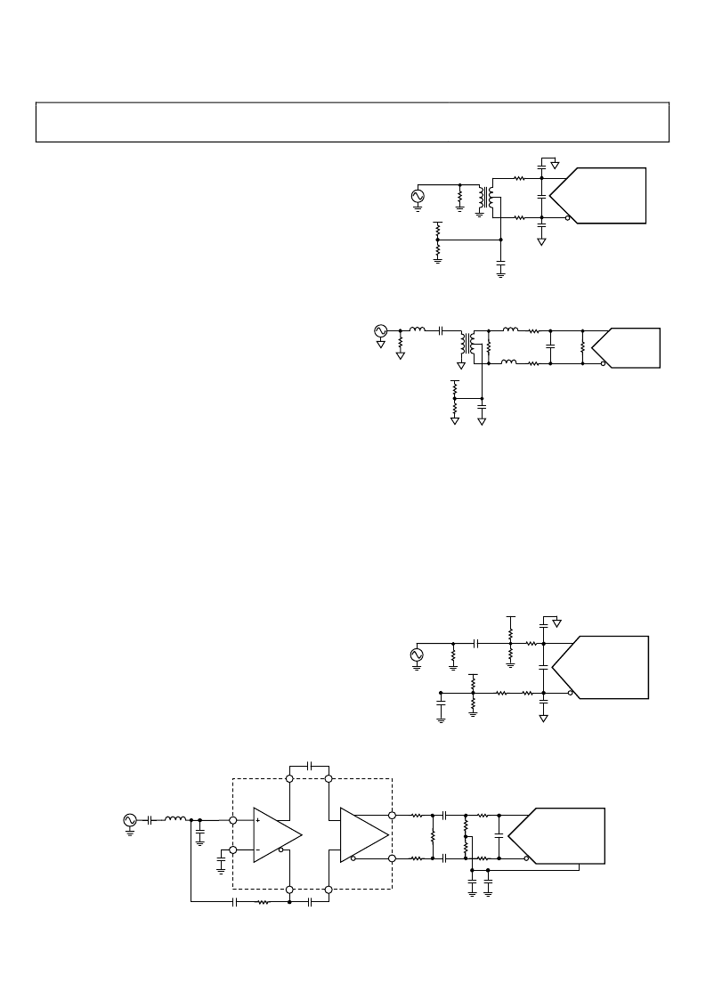
Differential Input Configurations
There are several ways in which to drive the AD9228 either
actively or passively. In either case, the optimum performance is
achieved by driving the analog input differentially. One example
is by using the
AD8332
differential driver. It provides excellent
performance and a flexible interface to the ADC (see Figure 49)
for baseband applications. This configuration is common for
medical ultrasound systems.
However, the noise performance of most amplifiers is not
adequate to achieve the true performance of the AD9228. For
applications where SNR is a key parameter, differential transfor-
mer coupling is the recommended input configuration. Two
examples are shown in Figure 46 and Figure 47.
In any configuration, the value of the shunt capacitor, C, is
dependent on the input frequency and may need to be reduced
or removed.
0
2Vp-p
R
R
*C
DIFF
C
*C
DIFF IS OPTIONAL
49.9
0.1
μ
F
1k
1k
AGND
AVDD
ADT1–1WT
1:1 Z RATIO
VIN–
ADC
AD9228
VIN+
C
Figure 46. Differential Transformer Coupled Configuration
for Baseband Applications
ADC
AD9228
VIN–
0
2Vp-p
2.2pF
33
1k
0.1
μ
F
1k
1k
AVDD
ADT1–1WT
1:1 Z RATIO
16nH
16nH
0.1
μ
F
16nH
33
499
65
VIN+
Figure 47. Differential Transformer Coupled Configuration for IF Applications
Single-Ended Input Configuration
A single-ended input may provide adequate performance in
cost-sensitive applications. In this configuration, SFDR and
distortion performance degrade due to the large input common-
mode swing. If the application requires a single-ended input
configuration, ensure that the source impedances on each input
are well matched in order to achieve the best possible performance.
A full-scale input of 2 V p-p can still be applied to the ADC’s VIN+
pin while the VIN pin is terminated. Figure 48 details a typical
single-ended input configuration.
0
2V p-p
R
R
49.9
0.1μF
0.1μF
AVDD
1k
25
1k
1k
AVDD
VIN–
ADC
AD9228
VIN+
*C
DIFF
C
*C
DIFF IS OPTIONAL
C
Figure 48. Single-Ended Input Configuration
AD8332
1.0k
1.0k
374
187
0
R
R
C
0.1
μ
F
187
0.1
μ
F
0.1
μ
F
0.1
μ
F
0.1
μ
F
10
μ
F
0.1
μ
F
1V p-p
0.1
μ
F
LNA
120nH
VGA
VOH
VIP
INH
22pF
LMD
VIN
LOP
LON
VOL
18nF
274
VIN–
ADC
AD9228
VIN+
VREF
Figure 49. Differential Input Configuration Using the
AD8332
相關PDF資料 |
PDF描述 |
|---|---|
| AD9228-65EB | Quad, 12-bit, 40/65 MSPS Serial LVDS 1.8 V A/D Converter |
| AD9229BCP-50 | Quad 12-Bit, 50/65 MSPS Serial LVDS 3V A/D Converter |
| AD9229BCP-65 | Quad 12-Bit, 50/65 MSPS Serial LVDS 3V A/D Converter |
| AD9229 | Quad 12-Bit, 50/65 MSPS Serial LVDS 3V A/D Converter |
| AD9235 | 12-Bit, 20/40/65 MSPS 3 V A/D Converter |
相關代理商/技術參數 |
參數描述 |
|---|---|
| AD9228_07 | 制造商:AD 制造商全稱:Analog Devices 功能描述:Quad, 12-Bit, 40/65 MSPS Serial LVDS 1.8 V A/D Converter |
| AD9228-65EB | 制造商:Analog Devices 功能描述: |
| AD9228-65EB1 | 制造商:AD 制造商全稱:Analog Devices 功能描述:High Speed ADC USB FIFO Evaluation Kit |
| AD9228-65EBZ | 功能描述:BOARD EVAL FOR AD9228 RoHS:是 類別:編程器,開發系統 >> 評估板 - 模數轉換器 (ADC) 系列:- 產品培訓模塊:Obsolescence Mitigation Program 標準包裝:1 系列:- ADC 的數量:1 位數:12 采樣率(每秒):94.4k 數據接口:USB 輸入范圍:±VREF/2 在以下條件下的電源(標準):- 工作溫度:-40°C ~ 85°C 已用 IC / 零件:MAX11645 已供物品:板,軟件 |
| AD9228ABCPZ-40 | 功能描述:IC ADC 12BIT SPI/SRL 40M 48LFCSP RoHS:是 類別:集成電路 (IC) >> 數據采集 - 模數轉換器 系列:- 其它有關文件:TSA1204 View All Specifications 標準包裝:1 系列:- 位數:12 采樣率(每秒):20M 數據接口:并聯 轉換器數目:2 功率耗散(最大):155mW 電壓電源:模擬和數字 工作溫度:-40°C ~ 85°C 安裝類型:表面貼裝 封裝/外殼:48-TQFP 供應商設備封裝:48-TQFP(7x7) 包裝:Digi-Reel® 輸入數目和類型:4 個單端,單極;2 個差分,單極 產品目錄頁面:1156 (CN2011-ZH PDF) 其它名稱:497-5435-6 |
發布緊急采購,3分鐘左右您將得到回復。