- 您現(xiàn)在的位置:買賣IC網(wǎng) > PDF目錄373968 > AD9802 (Analog Devices, Inc.) .50" x 50 Black/Clear 240 Industrial Label Supply RoHS Compliant: NA PDF資料下載
參數(shù)資料
| 型號(hào): | AD9802 |
| 廠商: | Analog Devices, Inc. |
| 英文描述: | .50" x 50 Black/Clear 240 Industrial Label Supply RoHS Compliant: NA |
| 中文描述: | CCD信號(hào)處理器電子照相機(jī) |
| 文件頁(yè)數(shù): | 4/20頁(yè) |
| 文件大小: | 366K |
| 代理商: | AD9802 |
第1頁(yè)第2頁(yè)第3頁(yè)當(dāng)前第4頁(yè)第5頁(yè)第6頁(yè)第7頁(yè)第8頁(yè)第9頁(yè)第10頁(yè)第11頁(yè)第12頁(yè)第13頁(yè)第14頁(yè)第15頁(yè)第16頁(yè)第17頁(yè)第18頁(yè)第19頁(yè)第20頁(yè)
AD9802
–4–
REV. 0
PIN FUNCT ION DE SCRIPT IONS
Pin #
1
2–11
12
13
14
15
16
17
18
19
20
21
22
23
24
25
26
27
28
29
30
31
32
33
34, 35
36
37
38
39
40
41
42
43
44, 45
46
47
48
Pin Name
ADVSS
D0–D9
DRVDD
DRVSS
DSUBST
DVSS
ADCCLK
DVDD
ST BY
PBLK
CLPOB
SHP
SHD
CLPDM
DVSS
CCDBYP2
DIN
PIN
CCDBYP1
PGACONT 1
PGACONT 2
ACVSS
CLAMP_BIAS
ACVDD
T EST 1, T EST 2
ADCIN
CMLEVEL
SHABYP
MODE2
MODE1
ADCMODE
NC
ADVDD
ADVSS
SUBST
VRB
VRT
T ype
P
DO
P
P
P
P
DI
P
DI
DI
DI
DI
DI
DI
P
AO
AI
AI
AO
AI
AI
P
AO
P
AI
AI
AO
AO
DI
DI
DI
Description
Analog Ground
Digital Data Outputs: D0 = LSB, D9 = MSB
+3 V Digital Driver Supply
Digital Driver Ground
Digital Substrate
Digital Ground
ADC Sample Clock Input
+3 V Digital Supply
Power-Down (Active High)
Pixel Blanking (Active Low)
Black Level Restore Clamp (Active Low)
Reference Sample Clock Input
Data Sample Clock Input
Input Clamp (Active Low)
Digital Ground
CCD Bypass. Decouple to analog ground through 0.1
μ
F.
CDS Input. T ie to Pin 27 and AC-Couple to CCD output through 0.1
μ
F.
CDS Input. See above.
CCD Bypass. Decouple to analog ground through 0.1
μ
F.
Coarse PGA Gain Control (0.3 V–2.7 V). Decoupled to analog ground through 0.1
μ
F.
Fine PGA Gain Control
Analog Ground
Clamp Bias Level. Decouple to analog ground through 0.1
μ
F.
+3 V Analog Supply
Reserved T est Pins. Should be left NC or pulled high to ACVDD.
Direct ADC Analog Input (See Driving the Direct ADC Input)
Common-Mode Level. Decouple to analog ground through 0.1
μ
F.
Internal Bias Level. Decouple to analog ground through 0.1
μ
F.
ADC T est Mode Control (See Digital Output Data Control.)
ADC T est Mode Control (See Digital Output Data Control.)
ADC Input Control. Logic low for CDS/PGA, high for direct input.
No Connect
+3 V Analog Supply
Analog Ground
Substrate. Connect to analog ground.
Bottom Reference Bypass. Decouple to analog ground through 0.1
μ
F.
T op Reference Bypass
P
P
P
AO
AO
NOT E
T ype: AI = Analog Input, AO = Analog Output, DI = Digital Input, DO = Digital Output, P = Power.
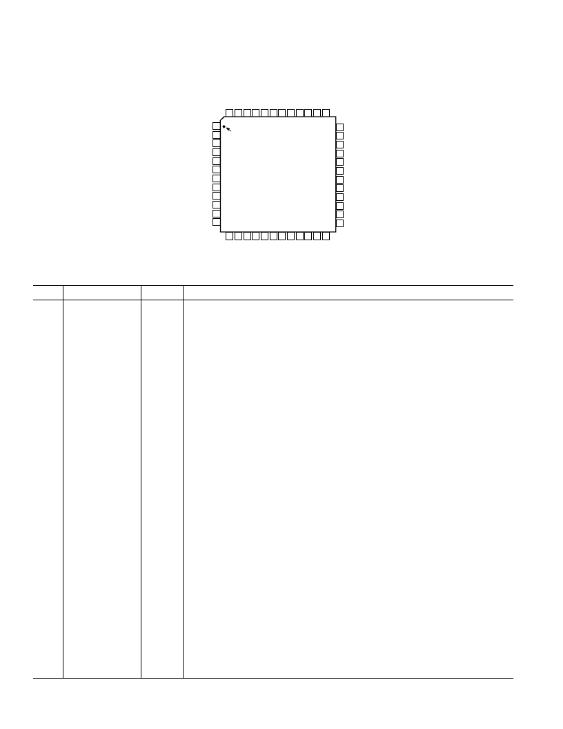
PIN CONFIGURAT ION
36
35
34
33
32
31
30
29
28
27
26
25
13 14 15 16 17 18 19 20 21 22 23 24
1
2
3
4
5
6
7
8
9
10
11
12
48 47 46 45 44
39 38 37
43 42 41 40
PIN 1
TOP VIEW
(Not to Scale)
D
D
D
A
S
ADVSS
(LSB) D0
D1
D2
D3
D4
D5
D6
D7
D8
(MSB) D9
DRVDD
NC = NO CONNECT
P
C
S
S
AD9802
D
ADCIN
TEST2
TEST1
ACVDD
CLAMP_BIAS
ACVSS
PGACONT2
PGACONT1
CCDBYP1
PIN
DIN
CCDBYP2
V
V
S
A
A
A
N
A
M
M
S
C
C
D
相關(guān)PDF資料 |
PDF描述 |
|---|---|
| AD9803 | CCD And Video Signal Processor For Electronic Cameras(電子照相機(jī)的CCD信號(hào)和視頻信號(hào)處理器) |
| AD9805 | Complete 12-Bit/10-Bit 6 MSPS CCD/CIS Signal Processors |
| AD9805JS | Complete 12-Bit/10-Bit 6 MSPS CCD/CIS Signal Processors |
| AD9807 | Complete 12-Bit/10-Bit 6 MSPS CCD/CIS Signal Processors |
| AD9807JS | Complete 12-Bit/10-Bit 6 MSPS CCD/CIS Signal Processors |
相關(guān)代理商/技術(shù)參數(shù) |
參數(shù)描述 |
|---|---|
| AD9802JST | 制造商:Rochester Electronics LLC 功能描述:- Bulk |
| AD9802JSTRL | 制造商:Rochester Electronics LLC 功能描述:- Tape and Reel |
| AD9803 | 制造商:AD 制造商全稱:Analog Devices 功能描述:CCD Signal Processor For Electronic Cameras |
| AD9803JST | 制造商:Rochester Electronics LLC 功能描述: |
| AD9803JST-28 | 制造商:Rochester Electronics LLC 功能描述:- Bulk |
發(fā)布緊急采購(gòu),3分鐘左右您將得到回復(fù)。