- 您現在的位置:買賣IC網 > PDF目錄373968 > AD9802 (Analog Devices, Inc.) .50" x 50 Black/Clear 240 Industrial Label Supply RoHS Compliant: NA PDF資料下載
參數資料
| 型號: | AD9802 |
| 廠商: | Analog Devices, Inc. |
| 英文描述: | .50" x 50 Black/Clear 240 Industrial Label Supply RoHS Compliant: NA |
| 中文描述: | CCD信號處理器電子照相機 |
| 文件頁數: | 8/20頁 |
| 文件大小: | 366K |
| 代理商: | AD9802 |
AD9802
–8–
REV. 0
T HE ORY OF OPE RAT ION
Introduction
T he AD9802 is a 10-bit analog-to-digital interface for CCD
cameras. T he block level diagram of the system is shown in
Figure 14. T he device includes a correlated double sampler
(CDS), 0 dB–31 dB variable gain amplifier (PGA), black level
correction loop, input clamp and voltage reference. T he only
external analog circuitry required at the system level is an emit-
ter follower buffer between the CCD output and AD9802
inputs.
CLAMP
CDS
BLACK
LEVEL
PGA
10-BIT
ADC
REF
OUT
GAIN
IN
Figure 14.
Correlated Double Sampling (CDS)
CDS is important in high performance CCD systems as a method
for removing several types of noise. Basically, two samples of the
CCD output are taken: one with the signal present (data) and one
without (reference). Subtracting these two samples removes
any noise that is common to—or correlates with—both.
Figure 15 shows the block diagram of the AD9802’s CDS. T he
S/H blocks are directly driven by the input and the sampling
function is performed passively, without the use of amplifiers.
T his implementation relies on the off-chip emitter follower
buffer to drive the two 10 pF sampling capacitors. Only one
capacitor at a time is seen at the input pin.
T he AD9802 actually uses two CDS circuits in a “ping-pong”
fashion to allow the system more acquisition time. In this way,
the output from one of the two CDS blocks will be valid for an
entire clock cycle. T hus, the bandwidth requirement of the
subsequent gain stage is reduced as compared to that for a
single CDS channel system. T his lower bandwidth translates to
lower power and noise.
10pF
Q1
S/H
Q2
S/H
S
OUT
FROM
CCD
Figure 15.
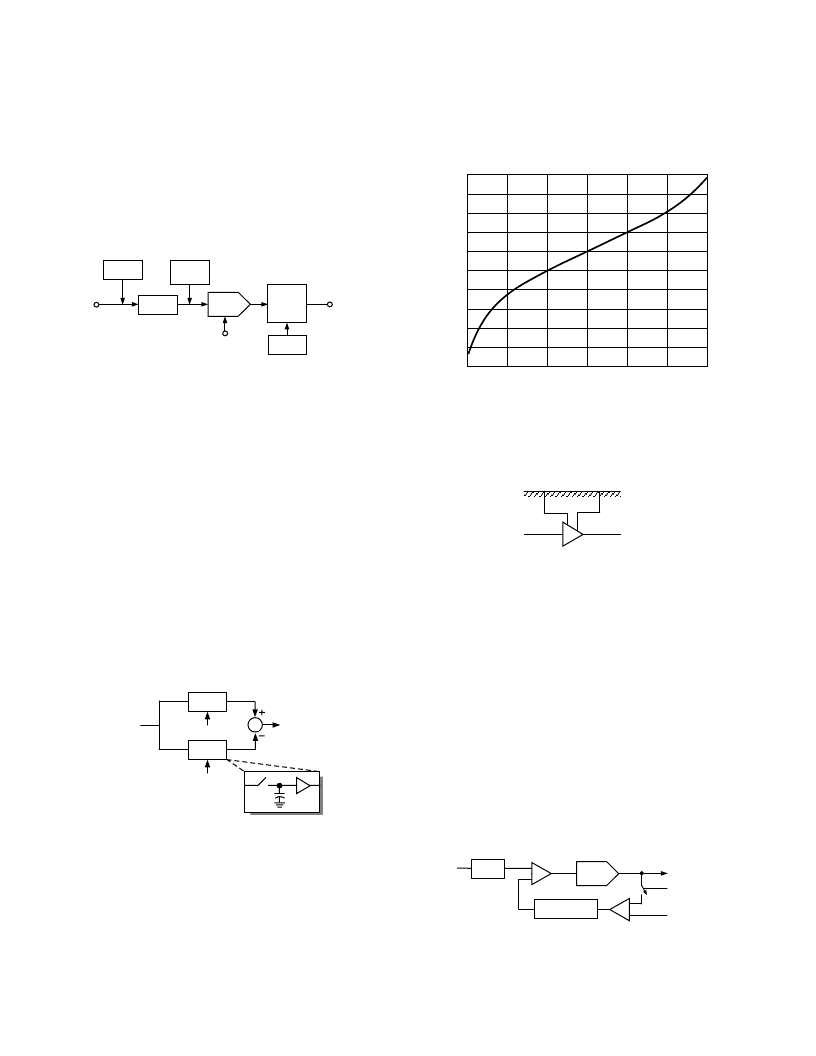
Programmable Gain Amplifier (PGA)
T he on-chip PGA provides a (linear in dB) gain range of 0 dB–
31.5 dB. A typical gain characteristic plot is shown in Figure 16.
Only the range from 0.3 V to 2.7 V is intended for actual use.
G
PGACONT1 – Volts
35
–15
0
3
0.5
1
1.5
2
2.5
30
15
0
–5
–10
25
20
10
5
Figure 16.
As shown in Figure 17, PGA control is provided through the
PGACONT 1 and PGACONT 2 inputs. PGACONT 1 provides
coarse, and PGACONT 2 fine (1/16), gain control.
A
PGACONT1
PGACONT2
PGACONT1 = COARSE CONTROL
PGACONT2 = FINE (1/16) CONTROL
Figure 17.
Black Level Clamping
For correct processing, the CCD signal must be referenced to a
well established “black level” by the AD9802. At the edge of the
CCD, there is a collection of pixels covered with metal to pre-
vent any light penetration. As the CCD is read out, these “black
pixels” provide a calibration signal that is used to establish the
black level.
T he feedback loop shown in Figure 18 is closed around the
PGA during the calibration interval (CLPOB = LOW) to set the
black level. As the black pixels are being processed, an integra-
tor block measures the difference between the input level and
the desired reference level. T his difference, or error, signal is
amplified and passed to the CDS block where it is added to the
incoming pixel data. As a result of this process, the black pixels
are digitized at one end of the ADC range, taking maximum
advantage of the available linear range of the system.
PGA
ADC
IN
CLPOB
NEG REF
INTEGRATOR
CDS
Figure 18.
相關PDF資料 |
PDF描述 |
|---|---|
| AD9803 | CCD And Video Signal Processor For Electronic Cameras(電子照相機的CCD信號和視頻信號處理器) |
| AD9805 | Complete 12-Bit/10-Bit 6 MSPS CCD/CIS Signal Processors |
| AD9805JS | Complete 12-Bit/10-Bit 6 MSPS CCD/CIS Signal Processors |
| AD9807 | Complete 12-Bit/10-Bit 6 MSPS CCD/CIS Signal Processors |
| AD9807JS | Complete 12-Bit/10-Bit 6 MSPS CCD/CIS Signal Processors |
相關代理商/技術參數 |
參數描述 |
|---|---|
| AD9802JST | 制造商:Rochester Electronics LLC 功能描述:- Bulk |
| AD9802JSTRL | 制造商:Rochester Electronics LLC 功能描述:- Tape and Reel |
| AD9803 | 制造商:AD 制造商全稱:Analog Devices 功能描述:CCD Signal Processor For Electronic Cameras |
| AD9803JST | 制造商:Rochester Electronics LLC 功能描述: |
| AD9803JST-28 | 制造商:Rochester Electronics LLC 功能描述:- Bulk |
發布緊急采購,3分鐘左右您將得到回復。