- 您現(xiàn)在的位置:買賣IC網(wǎng) > PDF目錄373968 > AD9822 (Analog Devices, Inc.) Complete 14-Bit CCD/CIS Signal Processor PDF資料下載
參數(shù)資料
| 型號(hào): | AD9822 |
| 廠商: | Analog Devices, Inc. |
| 英文描述: | Complete 14-Bit CCD/CIS Signal Processor |
| 中文描述: | 完整的14位防治荒漠化公約/ CIS信號(hào)處理器 |
| 文件頁數(shù): | 14/15頁 |
| 文件大小: | 150K |
| 代理商: | AD9822 |
REV. A
AD9822
–14–
28
27
26
25
24
23
22
21
20
19
18
17
16
15
1
2
3
4
5
6
7
8
9
10
11
12
13
14
AD9822
CDSCLK1
AVDD
CDSCLK2
ADCCLK
OEB
DRVDD
DRVSS
D7 (MSB)
D6
D5
D4
D3
D2
D1
D0 (LSB)
AVSS
VINR
OFFSET
VING
CML
VINB
CAPT
CAPB
AVSS
AVDD
SLOAD
SCLK
SDATA
3
CLOCK INPUTS
8
DATA OUTPUTS
0.1
m
F
3
SERIAL INTERFACE
0.1
m
F
5V/3V
5V
0.1
m
F
0.1
m
F
0.1
m
F
0.1
m
F
RED INPUT
GREEN INPUT
BLUE INPUT
0.1
m
F
0.1
m
F
1.0
m
F
10
m
F
0.1
m
F
+
0.1
m
F
5V
0.1
m
F
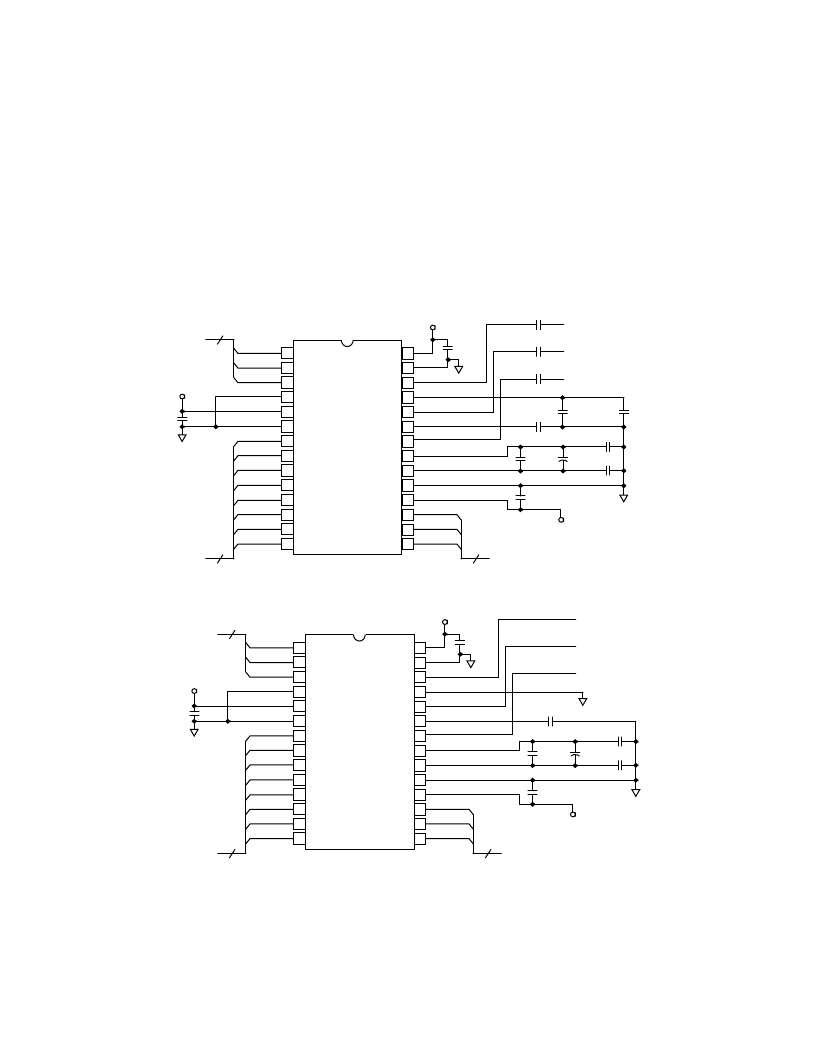
Figure 14. Recommended Circuit Configuration, 3-Channel CDS Mode
28
27
26
25
24
23
22
21
20
19
18
17
16
15
1
2
3
4
5
6
7
8
9
10
11
12
13
14
AD9822
CDSCLK1
AVDD
CDSCLK2
ADCCLK
OEB
DRVDD
DRVSS
D7 (MSB)
D6
D5
D4
D3
D2
D1
D0 (LSB)
AVSS
VINR
OFFSET
VING
CML
VINB
CAPT
CAPB
AVSS
AVDD
SLOAD
SCLK
SDATA
3
CLOCK INPUTS
8
DATA OUTPUTS
0.1
m
F
3
SERIAL INTERFACE
0.1
m
F
5V/3V
5V
0.1
m
F
RED INPUT
GREEN INPUT
BLUE INPUT
0.1
m
F
10
m
F
0.1
m
F
+
0.1
m
F
5V
0.1
m
F
Figure 15. Recommended Circuit Configuration, 3-Channel SHA Mode
(Analog Inputs Sampled with Respect to Ground)
APPLICATIONS INFORMATION
Circuit and Layout Recommendations
The recommended circuit configuration for 3-Channel CDS
mode operation is shown in Figure 14. The recommended input
coupling capacitor value is 0.1
μ
F (see Circuit Operation section
for more details). A single ground plane is recommended for the
AD9822. A separate power supply may be used for DRVDD,
the digital driver supply, but this supply pin should still be
decoupled to the same ground plane as the rest of the AD9822.
The loading of the digital outputs should be minimized, either
by using short traces to the digital ASIC, or by using external
digital buffers. To minimize the effect of digital transients during
major output code transitions, the falling edge of CDSCLK2
should occur coincident with or before the rising edge of
ADCCLK (see Figures 1 through 4 for timing). All 0.1
μ
F
decoupling capacitors should be located as close as possible to
the AD9822 pins. When operating in single channel mode, the
unused analog inputs should be grounded.
Figure 15 shows the recommended circuit configuration for 3-
Channel SHA mode. All of the above considerations also apply
for this configuration, except that the analog input signals are
directly connected to the AD9822 without the use of coupling
capacitors. The analog input signals must already be dc-biased
between 0 V and 2 V (see the Circuit Operation section for
more details).
相關(guān)PDF資料 |
PDF描述 |
|---|---|
| AD9822JR | Complete 14-Bit CCD/CIS Signal Processor |
| AD9822JRS | Complete 14-Bit CCD/CIS Signal Processor |
| AD9823 | Correlated Double Sampler (CDS) |
| AD9823BRUZ | Correlated Double Sampler (CDS) |
| AD9824KCP | Complete 14-Bit 30 MSPS CCD Signal Processor |
相關(guān)代理商/技術(shù)參數(shù) |
參數(shù)描述 |
|---|---|
| AD9822-EB | 制造商:Analog Devices 功能描述: |
| AD9822JR | 制造商:Analog Devices 功能描述:AFE Video 1ADC 14-Bit 5V 28-Pin SOIC W |
| AD9822JRRL | 制造商:Analog Devices 功能描述:AFE Video 1ADC 14-Bit 5V 28-Pin SOIC W T/R 制造商:Rochester Electronics LLC 功能描述:14 BIT AFE WITH 12 BIT LINEARITY - Bulk |
| AD9822JRS | 制造商:Analog Devices 功能描述:AFE Video 1ADC 14-Bit 5V 28-Pin SSOP |
| AD9822JRSRL | 制造商:Analog Devices 功能描述:AFE Video 1ADC 14-Bit 5V 28-Pin SSOP T/R 制造商:Rochester Electronics LLC 功能描述:14 BIT AFE WITH 12 BIT LINEARITY - Bulk |
發(fā)布緊急采購(gòu),3分鐘左右您將得到回復(fù)。