- 您現在的位置:買賣IC網 > PDF目錄373968 > AD9824KCP (ANALOG DEVICES INC) Complete 14-Bit 30 MSPS CCD Signal Processor PDF資料下載
參數資料
| 型號: | AD9824KCP |
| 廠商: | ANALOG DEVICES INC |
| 元件分類: | 模擬信號調理 |
| 英文描述: | Complete 14-Bit 30 MSPS CCD Signal Processor |
| 中文描述: | SPECIALTY ANALOG CIRCUIT, QCC48 |
| 封裝: | 7 X 7 MM, LFCSP-48 |
| 文件頁數: | 17/24頁 |
| 文件大小: | 438K |
| 代理商: | AD9824KCP |
REV. 0
AD9824
–17–
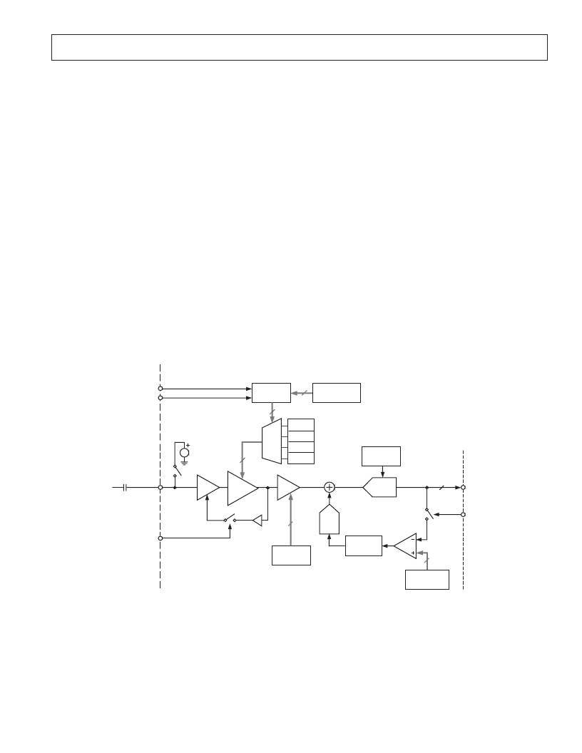
CIRCUIT DESCRIPTION AND OPERATION
The AD9824 signal processing chain is shown in Figure 25.
Each processing step is essential in achieving a high quality image
from the raw CCD pixel data.
DC Restore
To reduce the large dc offset of the CCD output signal, a dc
restore circuit is used with an external 0.1
μ
F series coupling
capacitor. This restores the dc level of the CCD signal to approxi-
mately 1.5 V to be compatible with the 3 V single supply of
the AD9824.
Correlated Double Sampler
The CDS circuit samples each CCD pixel twice to extract the
video information and reject low frequency noise. The timing
shown in Figure 5 illustrates how the two CDS clocks, SHP
and SHD, are used to sample the reference level and data level
of the CCD signal, respectively. The CCD signal is sampled on
the rising edges of SHP and SHD. Placement of these two clock
signals is critical in achieving the best performance from the CCD.
An internal SHP/SHD delay (t
ID
) of 3 ns is caused by internal
propagation delays.
Input Clamp
A line-rate input clamping circuit is used to remove the CCD’s
optical black offset. This offset exists in the CCD’s shielded black
reference pixels. Unlike some AFE architectures, the AD9824
removes this offset in the input stage to minimize the effect of a
gain change on the system black level. Another advantage of
removing this offset at the input stage is to maximize system
headroom. Some area CCDs have large black level offset volt-
ages, which, if not corrected at the input stage, can significantly
reduce the available headroom in the internal circuitry when
higher VGA gain settings are used.
Horizontal timing is shown in Figure 6. It is recommended
that the CLPDM pulse be used during valid CCD dark pixels.
CLPDM may be used during the optical black pixels, either
together with CLPOB or separately. The CLPDM pulse should
be a minimum of 4 pixels wide.
PxGA
The
PxGA
provides separate gain adjustment for the individual
color pixels. A programmable gain amplifier with four separate
values, the
PxGA
has the capability to “multiplex” its gain value
on a pixel-to-pixel basis. This allows lower output color pixels to
be gained up to match higher output color pixels. Also, the
PxGA
may be used to adjust the colors for white balance, reducing the
amount of digital processing that is needed. The four different gain
values are switched according to the color steering circuitry.
Seven different color steering modes for different types of CCD
color filter arrays are programmed in the AD9824’s Control Regis-
ter. For example, mosaic separate steering mode accommodates
the popular “Bayer” arrangement of red, green, and blue filters
(see Figure 26).
2dB TO 36dB
CLPDM
CCDIN
DIGITAL
FILTERING
CLPOB
DC RESTORE
OPTICAL BLACK
CLAMP
0.1 F
DOUT
14-BIT
ADC
VGA
8-BIT
DAC
CLAMP LEVEL
REGISTER
8
VGA GAIN
REGISTER
10
CDS
INPUT OFFSET
CLAMP
INTERNAL
V
REF
2V FULL SCALE
COLOR
STEERING
4:1
MUX
3
GAIN0
GAIN1
GAIN2
GAIN3
PxGA
–2dB TO +10dB
PxGA
MODE
SELECTION
2
6
VD
HD
PxGA
GAIN
REGISTERS
14
Figure 25. CCD Mode Block Diagram
相關PDF資料 |
PDF描述 |
|---|---|
| AD9824 | Complete 14-Bit 30 MSPS CCD Signal Processor |
| AD9826KRS | Complete 16-Bit Imaging Signal Processor |
| AD9826 | Complete 16-Bit Imaging Signal Processor |
| AD9830 | CMOS Complete DDS |
| AD9830AST | CMOS Complete DDS |
相關代理商/技術參數 |
參數描述 |
|---|---|
| AD9824KCPRL | 制造商:Analog Devices 功能描述:AFE Video 1ADC 14-Bit 3.3V 48-Pin LFCSP EP T/R |
| AD9824KCPZ | 功能描述:IC CCD SIGNAL PROC 14BIT 48LFCSP RoHS:是 類別:集成電路 (IC) >> 接口 - 傳感器和探測器接口 系列:- 其它有關文件:Automotive Product Guide 產品培訓模塊:Lead (SnPb) Finish for COTS Obsolescence Mitigation Program 標準包裝:74 系列:- 類型:觸控式傳感器 輸入類型:數字 輸出類型:數字 接口:JTAG,串行 電流 - 電源:100µA 安裝類型:表面貼裝 封裝/外殼:20-TSSOP(0.173",4.40mm 寬) 供應商設備封裝:20-TSSOP 包裝:管件 |
| AD9824KCPZ | 制造商:Analog Devices 功能描述:IC SEMICONDUCTOR ((NS)) |
| AD9824KCPZRL | 功能描述:IC CCD SIGNAL PROC 14BIT 48LFCSP RoHS:是 類別:集成電路 (IC) >> 接口 - 傳感器和探測器接口 系列:- 其它有關文件:Automotive Product Guide 產品培訓模塊:Lead (SnPb) Finish for COTS Obsolescence Mitigation Program 標準包裝:74 系列:- 類型:觸控式傳感器 輸入類型:數字 輸出類型:數字 接口:JTAG,串行 電流 - 電源:100µA 安裝類型:表面貼裝 封裝/外殼:20-TSSOP(0.173",4.40mm 寬) 供應商設備封裝:20-TSSOP 包裝:管件 |
| AD9826 | 制造商:AD 制造商全稱:Analog Devices 功能描述:Complete 16-Bit Imaging Signal Processor |
發布緊急采購,3分鐘左右您將得到回復。