- 您現在的位置:買賣IC網 > PDF目錄373969 > AD9858TLPCB (Analog Devices, Inc.) 1 GSPS Direct Digital Synthesizer PDF資料下載
參數資料
| 型號: | AD9858TLPCB |
| 廠商: | Analog Devices, Inc. |
| 元件分類: | XO, clock |
| 英文描述: | 1 GSPS Direct Digital Synthesizer |
| 中文描述: | 1 GSPS的直接數字頻率合成器 |
| 文件頁數: | 8/32頁 |
| 文件大小: | 1412K |
| 代理商: | AD9858TLPCB |
第1頁第2頁第3頁第4頁第5頁第6頁第7頁當前第8頁第9頁第10頁第11頁第12頁第13頁第14頁第15頁第16頁第17頁第18頁第19頁第20頁第21頁第22頁第23頁第24頁第25頁第26頁第27頁第28頁第29頁第30頁第31頁第32頁

AD9858
PIN FUNCTION DESCRIPTIONS
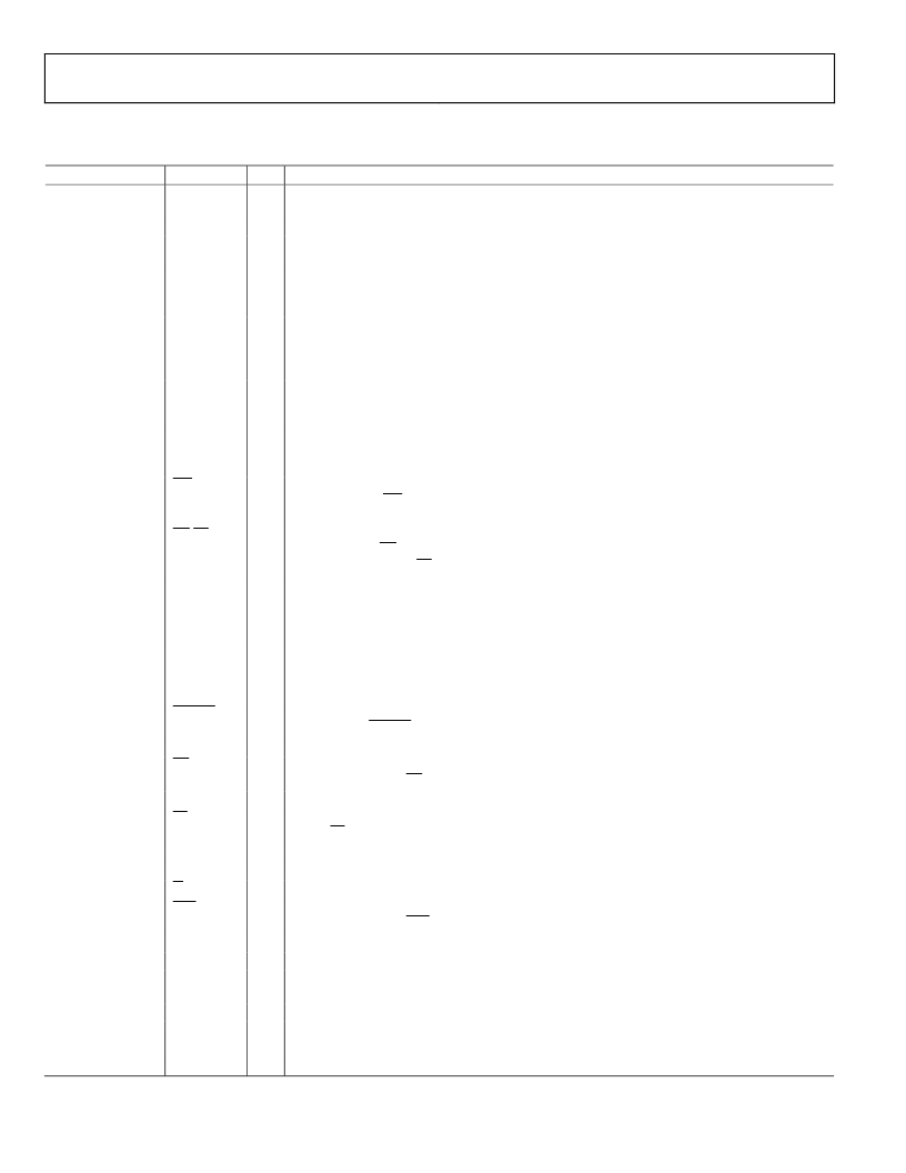
Table 4. Pin Function Descriptions—100-Lead EPAD (SV-100)
Pin No.
Mnemonic
1 to 4, 9 to 12
D7 to D0
Rev. A | Page 8 of 32
I/O
I
Description
Parallel Port DATA. Note that the functionality of these pins is valid only when the I/O port is
configured as a parallel port.
Digitial Ground.
Digital Supply Voltage.
5, 6, 21, 28, 95, 96
7, 8, 20,
23 to 27, 93, 94
13 to 18
DGND
DVDD
ADDR5 to
ADDR0
I
When the I/O port is configured as a parallel port, these pins serve as a 6-bit address select
for accessing the on-chip registers (see the IORESET, SDO, and SDIO pins below for serial
port mode).
Note that this is valid only for serial programming mode. Active high input signal that resets the
serial I/O bus controller. It is intended to serve as a means of recovering from an unresponsive
serial bus caused by improper programming protocol. Asserting an I/O reset does not affect the
contents of previously programmed registers nor does it invoke their default values.
Note that this is valid only for serial programming mode. When operating the I/O port as a
3-wire serial port, this pin serves as a unidirectional serial data output pin. When operated as a
2-wire serial port, this pin is unused.
Note that this is valid only for serial programming mode. When operating the I/O port as a
3-wire serial port, this pin is the serial data input. When operated as a 2-wire serial port, this pin
is the bidirectional serial data pin.
When the I/O port is configured for parallel programming mode, this pin functions as an active
low write pulse (WR). When configured for serial programming mode, this pin functions as the
serial data clock (SCLK).
When the I/O port is configured for parallel programming mode, this pin functions as an active
low read pulse (RD). When configured for serial programming mode, this pin functions as an
active low chip select (CS) that allows multiple devices to share the serial bus.
Analog Ground.
16
IORESET
I
17
SDO
O
18
SDIO
I or
I/O
19
WR/SCLK
I
22
RD/CS
I
29, 30, 37 to 39,
41, 42, 49, 50,
52, 69, 74, 80, 85,
87, 88
31, 32, 35, 36,
40, 43, 44, 47,
48, 51, 70, 73,
77, 86, 89, 90
33
AGND
I
AVDD
I
Analog Supply Voltage.
REFCLK
I
Reference Clock Complementary Input. (Note that when the REFCLK port is operated in single-
ended mode, REFCLK should be decoupled to AVDD with a 0.1 μF capacitor.
Reference Clock Input.
Mixer Local Oscillator (LO) Complementary Input. Note that when the LO port is operated in
single-ended mode, LO should be decoupled to AVDD with a 0.1 μF capacitor.
Mixer Local Oscillator (LO) Input.
Analog Mixer RF Complementary Input. Note that when the RF port is operated in single-ended
mode, RF should be decoupled to AVDD with a 0.1 μF capacitor.
Analog Mixer RF Input.
Analog Mixer IF Output.
Analog Mixer IF Complementary Output.
Phase Frequency Detector Complementary Input . Note that when the PFD port is operated in
single-ended mode, PFD should be decoupled to AVDD with a 0.1 μF capacitor.
Phase Frequency Detector Input.
No Connection.
Charge Pump Output Current Control. A resistor connected from CPISET to CPGND establishes
the reference current for the charge pump.
Charge Pump Supply Voltage.
Charge Pump Ground.
Charge Pump Fast Lock Output.
Charge Pump Output.
34
45
REFCLK
LO
I
I
46
53
LO
RF
I
I
54
55
56
57
RF
IF
IF
PFD
I
O
O
I
58
59, 60, 75, 76
61
PFD
NC
CPISET
I
I
62, 67
63, 68
64
65, 66
CPVDD
CPGND
CPFL
CP
I
I
O
O
相關PDF資料 |
PDF描述 |
|---|---|
| AD9858BSV | 1 GSPS Direct Digital Synthesizer |
| AD9858PCB | 1 GSPS Direct Digital Synthesizer |
| AD9858 | 1 GSPS Direct Digital Synthesizer |
| AD9858FDPCB | 1 GSPS Direct Digital Synthesizer |
| AD9859 | 400 MSPS, 10-Bit, 1.8 V CMOS Direct Digital Synthesizer |
相關代理商/技術參數 |
參數描述 |
|---|---|
| AD9858XSV | 制造商:Analog Devices 功能描述: |
| AD9859 | 制造商:AD 制造商全稱:Analog Devices 功能描述:400 MSPS, 10-Bit, 1.8 V CMOS Direct Digital Synthesizer |
| AD9859/PCB | 制造商:Analog Devices 功能描述:NCO, 400MSPS 10 BIT, 1.8V CMOS DIRECT DGTL SYNTHESIZER - Bulk |
| AD9859/PCBZ | 功能描述:BOARD EVAL FOR AD9859 RoHS:是 類別:編程器,開發系統 >> 評估演示板和套件 系列:AgileRF™ 標準包裝:1 系列:- 主要目的:電信,線路接口單元(LIU) 嵌入式:- 已用 IC / 零件:IDT82V2081 主要屬性:T1/J1/E1 LIU 次要屬性:- 已供物品:板,電源,線纜,CD 其它名稱:82EBV2081 |
| AD9859/PCBZ1 | 制造商:AD 制造商全稱:Analog Devices 功能描述:400 MSPS, 10-Bit,1.8 V CMOS Direct Digital Synthesizer |
發布緊急采購,3分鐘左右您將得到回復。