- 您現在的位置:買賣IC網 > PDF目錄373973 > AD9995KCP (ANALOG DEVICES INC) 12-Bit CCD Signal Processor with Precision Timing ⑩ Generator PDF資料下載
參數資料
| 型號: | AD9995KCP |
| 廠商: | ANALOG DEVICES INC |
| 元件分類: | 消費家電 |
| 英文描述: | 12-Bit CCD Signal Processor with Precision Timing ⑩ Generator |
| 中文描述: | SPECIALTY CONSUMER CIRCUIT, QCC56 |
| 封裝: | 8 X 8 MM, MO-220-VLLD-2, LFCSP-56 |
| 文件頁數: | 13/60頁 |
| 文件大小: | 1593K |
| 代理商: | AD9995KCP |
第1頁第2頁第3頁第4頁第5頁第6頁第7頁第8頁第9頁第10頁第11頁第12頁當前第13頁第14頁第15頁第16頁第17頁第18頁第19頁第20頁第21頁第22頁第23頁第24頁第25頁第26頁第27頁第28頁第29頁第30頁第31頁第32頁第33頁第34頁第35頁第36頁第37頁第38頁第39頁第40頁第41頁第42頁第43頁第44頁第45頁第46頁第47頁第48頁第49頁第50頁第51頁第52頁第53頁第54頁第55頁第56頁第57頁第58頁第59頁第60頁
AD9995
–13–
HORIZONTAL CLAMPING AND BLANKING
The AD9995’s horizontal clamping and blanking pulses are fully
programmable to suit a variety of applications. Individual control
is provided for CLPOB, PBLK, and HBLK during the different
regions of each field. This allows the dark pixel clamping and
blanking patterns to be changed at each stage of the readout in
order to accommodate different image transfer timing and high
speed line shifts.
Individual CLPOB and PBLK Patterns
The AFE horizontal timing consists of CLPOB and PBLK, as
shown in Figure 9. These two signals are independently pro-
grammed using the registers in Table III. SPOL is the start
polarity for the signal, and TOG1 and TOG2 are the first and
second toggle positions of the pulse. Both signals are active low
and should be programmed accordingly.
A separate pattern for CLPOB and PBLK may be programmed
for every 10 V-sequences. As described in the Vertical Timing
Generation section, up to 10 separate V-sequences can be created,
each containing a unique pulse pattern for CLPOB and PBLK.
Figure 9 shows how the sequence change positions divide the
readout field into different regions. A different V-sequence can be
assigned to each region, allowing the CLPOB and PBLK signals
to be changed accordingly with each change in the vertical timing.
Individual HBLK Patterns
The HBLK programmable timing shown in Figure 10 is simi-
lar to CLPOB and PBLK. However, there is no start polarity
control. Only the toggle positions are used to designate the start
and stop positions of the blanking period. Additionally, there is a
polarity control HBLKMASK that designates the polarity of the
horizontal clock signals H1–H4 during the blanking period. Set-
ting HBLKMASK high will set H1 = H3 = low and H2 = H4 =
high during the blanking, as shown in Figure 11. As with the
CLPOB and PBLK signals, HBLK registers are available in each
V-sequence, allowing different blanking signals to be used with
different vertical timing sequences.
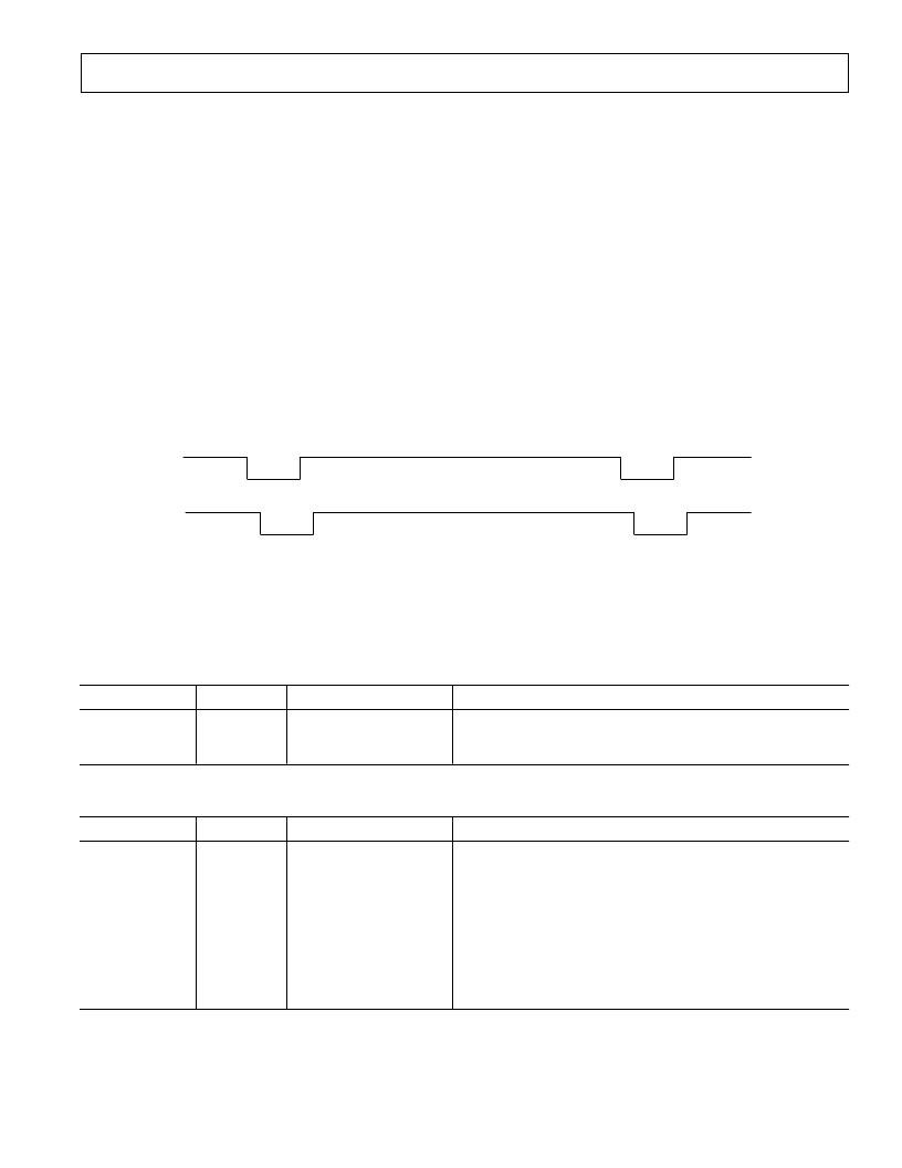
(3)
(2)
(1)
HD
CLPOB
PBLK
. . .
NOTES
PROGRAMMABLE SETTINGS:
1. START POLARITY (CLAMP AND BLANK REGION ARE ACTIVE LOW)
2. FIRST TOGGLE POSITION
3. SECOND TOGGLE POSITION
. . .
ACTIVE
ACTIVE
Figure 9. Clamp and Pre-Blank Pulse Placement
Table III. CLPOB and PBLK Pattern Registers
Range
High/Low
0–4095 Pixel Location
0–4095 Pixel Location
Register
SPOL
TOG1
TOG2
Length
1b
12b
12b
Description
Starting Polarity of CLPOB/PBLK for V-Sequence 0–9
First Toggle Position within Line for V-Sequence 0–9
Second Toggle Position within Line for V-Sequence 0–9
Table IV. HBLK Pattern Registers
Register
HBLKMASK
HBLKALT
HBLKTOG1
HBLKTOG2
HBLKTOG3
HBLKTOG4
HBLKTOG5
HBLKTOG6
Length
1b
2b
12b
12b
12b
12b
12b
12b
Range
High/Low
0–3 Alternation Mode
0–4095 Pixel Location
0–4095 Pixel Location
0–4095 Pixel Location
0–4095 Pixel Location
0–4095 Pixel Location
0–4095 Pixel Location
Description
Masking Polarity for H1/H3 (0 = H1/H3 Low, 1 = H1/H3 High)
Enables Odd/Even Alternation of HBLK Toggle Positions 0 =
Disable Alternation. 1 = TOG1–TOG2 Odd, TOG3–TOG6 Even.
2 = 3 = TOG1–TOG2 Even, TOG3–TOG6 Odd
First Toggle Position within Line for Each V-Sequence 0–9
Second Toggle Position within Line for Each V-Sequence 0–9
Third Toggle Position within Line for Each V-Sequence 0–9
Fourth Toggle Position within Line for Each V-Sequence 0–9
Fifth Toggle Position within Line for Each V-Sequence 0–9
Sixth Toggle Position within Line for Each V-Sequence 0–9
REV. 0
相關PDF資料 |
PDF描述 |
|---|---|
| AD9995KCPRL | 12-Bit CCD Signal Processor with Precision Timing ⑩ Generator |
| AD9995 | 12-Bit CCD Signal Processor with Precision Timing ⑩ Generator |
| ADA4000-2ARMZ-RL | Low Cost, Precision JFET Input Operational Amplifiers |
| ADA4000-1 | Low Cost, Precision JFET Input Operational Amplifiers |
| ADA4000-1_07 | Low Cost, Precision JFET Input Operational Amplifiers |
相關代理商/技術參數 |
參數描述 |
|---|---|
| AD9995KCPRL | 制造商:Analog Devices 功能描述:AFE Video 1ADC 12-Bit 3V 56-Pin LFCSP EP T/R 制造商:Rochester Electronics LLC 功能描述:- Bulk |
| AD9995KCPZ | 功能描述:IC CCD SIGNAL PROCESSOR 56-LFCSP RoHS:是 類別:集成電路 (IC) >> 接口 - 傳感器和探測器接口 系列:- 其它有關文件:Automotive Product Guide 產品培訓模塊:Lead (SnPb) Finish for COTS Obsolescence Mitigation Program 標準包裝:74 系列:- 類型:觸控式傳感器 輸入類型:數字 輸出類型:數字 接口:JTAG,串行 電流 - 電源:100µA 安裝類型:表面貼裝 封裝/外殼:20-TSSOP(0.173",4.40mm 寬) 供應商設備封裝:20-TSSOP 包裝:管件 |
| AD9995KCPZRL | 功能描述:IC CCD SIGNAL PROCESSOR 56-LFCSP RoHS:是 類別:集成電路 (IC) >> 接口 - 傳感器和探測器接口 系列:- 其它有關文件:Automotive Product Guide 產品培訓模塊:Lead (SnPb) Finish for COTS Obsolescence Mitigation Program 標準包裝:74 系列:- 類型:觸控式傳感器 輸入類型:數字 輸出類型:數字 接口:JTAG,串行 電流 - 電源:100µA 安裝類型:表面貼裝 封裝/外殼:20-TSSOP(0.173",4.40mm 寬) 供應商設備封裝:20-TSSOP 包裝:管件 |
| AD9995KCPZRL7 | 制造商:Rochester Electronics LLC 功能描述: 制造商:Analog Devices 功能描述: |
| AD9996BBCZ | 制造商:Rochester Electronics LLC 功能描述:14B 40 MSPS AFETG CONVERTER - Bulk |
發布緊急采購,3分鐘左右您將得到回復。