- 您現在的位置:買賣IC網 > PDF目錄373975 > ADC912AFS (ANALOG DEVICES INC) CMOS Microprocessor-Compatible 12-Bit A/D Converter PDF資料下載
參數資料
| 型號: | ADC912AFS |
| 廠商: | ANALOG DEVICES INC |
| 元件分類: | ADC |
| 英文描述: | CMOS Microprocessor-Compatible 12-Bit A/D Converter |
| 中文描述: | 1-CH 12-BIT SUCCESSIVE APPROXIMATION ADC, PARALLEL ACCESS, PDSO24 |
| 封裝: | SOIC-24 |
| 文件頁數: | 10/16頁 |
| 文件大小: | 237K |
| 代理商: | ADC912AFS |
REV. B
ADC912A
–10–
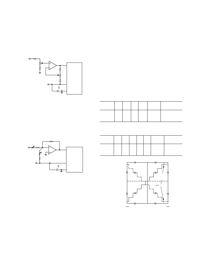
BIPOLAR ANALOG INPUT OPERATION
Bipolar analog input operation is achieved with an external
amplifier providing an analog offset. Figures 17 and 18 show
two circuit topologies that result in different digital-output cod-
ing. In Figure 17, offset binary coding is produced when the
external amplifier is connected in the inverting mode. Figure 19
shows the ideal transfer characteristics for both the inverting
and noninverting configurations given in Figures 17 and 18.
AGND
V
REFIN
A
IN
0.1 F 10 F
1
2
–
5V
R2
R1
R3
R4
R
FS
R
Z
V
IN
3
R1 = R2 = 20k
SEE TABLE II FOR VALUES OF R3, R4, R
, AND R
FS
A1: OP27 LOWEST NOISE, OP42 BEST BANDWIDTH
*
EXTRA PINS OMITTED FOR CLARITY
ADC912A
*
A1
Figure 17. Noninverting Bipolar Analog Input Operation
The scaling resistors chosen in bipolar input applications should
be from the same manufacturer to obtain good resistor tracking
performance over temperature. When potentiometers are used
for absolute adjustment, 0.1% tolerance resistors should still be
used as shown in Figures 17 and 18 to minimize temperature
coefficient errors.
–
5V
0.1 F
10 F
+
2
3AGND
V
REFIN
A
IN
V
IN
1
R1
R2
R3
R
FS
R
Z
SEE TABLE III FOR VALUES OF R1, R2, R3, R4, R
, AND R
FS
A1: OP27 LOWEST NOISE, OP42 BEST BANDWIDTH
*
EXTRA PINS OMITTED FOR CLARITY
ADC912A
*
A1
Figure 18. Inverting Bipolar Analog Input
Calibration of the bipolar analog input circuits (Figures 17 and
18) should begin with zero adjustment first. Apply a +1/2 LSB
analog input to A
IN
, (see Tables II and III) and adjust R
Z
until the
successive digital output codes flicker between the following codes:
For noninverting, Figure 17
1000 0000 0000
1000 0000 0001
0111 1111 1111
0111 1111 1110
For inverting, Figure 18
Next, adjust full scale by applying a FS–3/2 LSB analog input to
A
IN
, (see Tables II and III) and adjust R
FS
until the successive
digital output codes flicker between the following codes:
For Noninverting, Figure 17
1111 1111 1110
1111 1111 1111
0000 0000 0001
0000 0000 0000
For Inverting, Figure 18
Table II. Resistor and Potentiometer Values Required for
Figure 17
V
IN
Range
V
R3
k
R4
k
R
Z
k
R
FS
k
1/2 LSB
mV
FS/2–3/2 LSB
V
±
2.5
±
5.0
±
10.0
0
20.0
29.8
40.2
19.8
10.0
0.5
0.5
0.5
0.5
1.0
0.5
0.61
1.22
2.44
2.49817
4.99634
9.99268
Table III. Resistor and Potentiometer Values Required for
Figure 18
V
IN
Range
V
R1
k
R2
k
R3
k
R
Z
k
R
FS
k
1/2 LSB
mV
FS/2–3/2 LSB
V
±
2.5
±
5.0
±
10.0
20.0
20.0
20.0
41.2
20.5
10.5
40.2 2
20.0 1
10.2 0.5
1
1
1
0.61
1.22
2.44
2.49817
4.99634
9.99268
111...110
100...000
111...111
100...001
011...111
011...110
000...001
000...000
DIGITAL OUTPUT
0V
FS
2
–
FS
2
+
INVERTING
FIGURE 18
V
IN
–
Input Voltage
FS
2
+
–
1LSB
NON-
INVERTING
FIGURE 17
Figure 19. Ideal Input/Output Transfer Characteristics for
Bipolar Input Circuits
相關PDF資料 |
PDF描述 |
|---|---|
| ADCMP341 | Dual 0.275% Comparators and Reference with Programmable Hysteresis |
| ADCMP341_07 | Dual 0.275% Comparators and Reference with Programmable Hysteresis |
| ADCMP341YRJZ-REEL7 | Dual 0.275% Comparators and Reference with Programmable Hysteresis |
| ADCMP343 | Dual 0.275% Comparators and Reference with Programmable Hysteresis |
| ADCMP343YRJZ-REEL7 | Dual 0.275% Comparators and Reference with Programmable Hysteresis |
相關代理商/技術參數 |
參數描述 |
|---|---|
| ADC-914MC | 功能描述:模數轉換器 - ADC Analog to Digital Converter RoHS:否 制造商:Texas Instruments 通道數量:2 結構:Sigma-Delta 轉換速率:125 SPs to 8 KSPs 分辨率:24 bit 輸入類型:Differential 信噪比:107 dB 接口類型:SPI 工作電源電壓:1.7 V to 3.6 V, 2.7 V to 5.25 V 最大工作溫度:+ 85 C 安裝風格:SMD/SMT 封裝 / 箱體:VQFN-32 |
| ADC-914MM | 制造商:未知廠家 制造商全稱:未知廠家 功能描述:Analog-to-Digital Converter, 14-Bit |
| ADC9708 | 制造商:未知廠家 制造商全稱:未知廠家 功能描述: |
| ADC9708CCJ | 制造商:NSC 制造商全稱:National Semiconductor 功能描述:6-Channel 8-Bit uP Compatible A/D Converter |
| ADC9708CCN | 制造商:NSC 制造商全稱:National Semiconductor 功能描述:6-Channel 8-Bit uP Compatible A/D Converter |
發布緊急采購,3分鐘左右您將得到回復。