- 您現(xiàn)在的位置:買(mǎi)賣(mài)IC網(wǎng) > PDF目錄373975 > ADC912AFS (ANALOG DEVICES INC) CMOS Microprocessor-Compatible 12-Bit A/D Converter PDF資料下載
參數(shù)資料
| 型號(hào): | ADC912AFS |
| 廠商: | ANALOG DEVICES INC |
| 元件分類(lèi): | ADC |
| 英文描述: | CMOS Microprocessor-Compatible 12-Bit A/D Converter |
| 中文描述: | 1-CH 12-BIT SUCCESSIVE APPROXIMATION ADC, PARALLEL ACCESS, PDSO24 |
| 封裝: | SOIC-24 |
| 文件頁(yè)數(shù): | 12/16頁(yè) |
| 文件大小: | 237K |
| 代理商: | ADC912AFS |
第1頁(yè)第2頁(yè)第3頁(yè)第4頁(yè)第5頁(yè)第6頁(yè)第7頁(yè)第8頁(yè)第9頁(yè)第10頁(yè)第11頁(yè)當(dāng)前第12頁(yè)第13頁(yè)第14頁(yè)第15頁(yè)第16頁(yè)
REV. B
ADC912A
–12–
CIRCUIT LAYOUT GUIDELINES
As with any high-speed A/D converters, good circuit layout
practice is essential. Wire-wrap boards are not recommended
due to stray pickup of the high-frequency digital noise. A PC
board offers the best results. Digital and analog grounds
should be separated even if they are ground planes instead of
ground traces. Do not lay digital traces adjacent to high-
impedance analog traces. Avoid digital layouts that radiate
high-frequency clock signals; i.e., do not lay out digital signal
lines and ground returns in the shape of a loop antenna. Shield
the analog input if it comes from a different PC board source.
Set up a single point ground at AGND (Pin 3) of the ADC912A;
tie all other analog grounds to this point. Also tie the logic
power supply ground, but no other digital grounds, to this point
(see Figure 21). Low impedance analog and digital power sup-
ply common returns are essential to low noise operation of the
ADC. Their trace widths should be as wide as possible. Good
power supply bypass capacitors located near the ADC package
ensure quiet operation. Place a 10
μ
F capacitor in parallel with a
0.01
μ
F ceramic capacitor across V
DD
to ground and V
SS
to
ground (near Pin 3).
COMMON
GROUND
ANALOG
CIRCUITS
AGND
V
SS
DGND
V
DD
+15V
GND
–
15V
ADC912A
DIGITAL
CIRCUITS
ANALOG
SUPPLY
DIGITAL
SUPPLY
RETURN
+5V
Figure 21. Power Supply Grounding
In applications where the ADC912A data outputs and control
signals are connected to a continuously active microprocessor
bus, it is possible to get LSB level errors in conversion results.
These errors are due to a feedthrough from the microprocessor
to the internal comparator. The problem can be minimized by
forcing the microprocessor into a WAIT state during conversion
(see Slow-Memory microprocessor interfacing). An alternate
method is isolation of the data bus with three-state buffers, such
as the 74HC541.
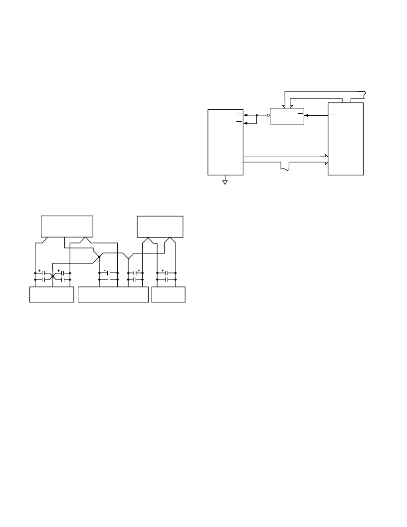
INTERFACING TO THE TMS32010 DSP PROCESSOR
Figure 22 shows an ADC912A to TMS32010 interface. The
ADC912A is operating in the ROM mode. The interface
is designed for the maximum TMS32010 clock frequency
of 20 MHz.
ADDRESS
DECODE
ADDRESS BUS
DATA BUS
PA
0
PA
2
D
15
D
0
D
11
D
0/8
HBEN
ADC912A
*
TMS32010
*
CS
RD
DEN
EN
*
ESSENTIAL INTERFACE CIRCUITRY SHOWN FOR CLARITY
Figure 22. ADC912A to TMS32010 DSP Processor Interface
The ADC912A is mapped at a user-selected port address (PA).
The following I/O instruction starts a conversion and reads the
previous conversion into the data memory:
IN DATA, PA
PA = Port Address
DATA = Data Memory Location
When conversion is complete, a second I/O instruction reads the
new data into the data memory and starts another conversion.
Sufficient A/D conversion time must be allowed between I/O
instructions. The very first data read after system power-up
should be discarded.
USING WAIT STATES
The TMS32020 DSP processor has the added capability of
WAIT states. This feature simplifies the hardware required for
slow memory devices by extending the microprocessor bus
access time. Figure 23 shows an ADC912A to TMS32020
interface using one WAIT state to guarantee data interface at
the full 20 MHz clock frequency. This WAIT state extends the
bus access time by 200 ns. In this circuit the ADC912A operated
in the ROM mode where each input instruction (IN DATA, PA)
takes the previous conversion result and stores it in memory. The
next input instruction must be delayed for the length of the A/D
conversion time so that a new conversion result can be read.
相關(guān)PDF資料 |
PDF描述 |
|---|---|
| ADCMP341 | Dual 0.275% Comparators and Reference with Programmable Hysteresis |
| ADCMP341_07 | Dual 0.275% Comparators and Reference with Programmable Hysteresis |
| ADCMP341YRJZ-REEL7 | Dual 0.275% Comparators and Reference with Programmable Hysteresis |
| ADCMP343 | Dual 0.275% Comparators and Reference with Programmable Hysteresis |
| ADCMP343YRJZ-REEL7 | Dual 0.275% Comparators and Reference with Programmable Hysteresis |
相關(guān)代理商/技術(shù)參數(shù) |
參數(shù)描述 |
|---|---|
| ADC-914MC | 功能描述:模數(shù)轉(zhuǎn)換器 - ADC Analog to Digital Converter RoHS:否 制造商:Texas Instruments 通道數(shù)量:2 結(jié)構(gòu):Sigma-Delta 轉(zhuǎn)換速率:125 SPs to 8 KSPs 分辨率:24 bit 輸入類(lèi)型:Differential 信噪比:107 dB 接口類(lèi)型:SPI 工作電源電壓:1.7 V to 3.6 V, 2.7 V to 5.25 V 最大工作溫度:+ 85 C 安裝風(fēng)格:SMD/SMT 封裝 / 箱體:VQFN-32 |
| ADC-914MM | 制造商:未知廠家 制造商全稱(chēng):未知廠家 功能描述:Analog-to-Digital Converter, 14-Bit |
| ADC9708 | 制造商:未知廠家 制造商全稱(chēng):未知廠家 功能描述: |
| ADC9708CCJ | 制造商:NSC 制造商全稱(chēng):National Semiconductor 功能描述:6-Channel 8-Bit uP Compatible A/D Converter |
| ADC9708CCN | 制造商:NSC 制造商全稱(chēng):National Semiconductor 功能描述:6-Channel 8-Bit uP Compatible A/D Converter |
發(fā)布緊急采購(gòu),3分鐘左右您將得到回復(fù)。