- 您現(xiàn)在的位置:買賣IC網(wǎng) > PDF目錄373982 > ADF4193 (Analog Devices, Inc.) Low Phase Noise, Fast Settling PLL Frequency Synthesizer PDF資料下載
參數(shù)資料
| 型號(hào): | ADF4193 |
| 廠商: | Analog Devices, Inc. |
| 英文描述: | Low Phase Noise, Fast Settling PLL Frequency Synthesizer |
| 中文描述: | 低相位噪聲,快速設(shè)置的鎖相環(huán)頻率合成器 |
| 文件頁數(shù): | 6/28頁 |
| 文件大小: | 437K |
| 代理商: | ADF4193 |
第1頁第2頁第3頁第4頁第5頁當(dāng)前第6頁第7頁第8頁第9頁第10頁第11頁第12頁第13頁第14頁第15頁第16頁第17頁第18頁第19頁第20頁第21頁第22頁第23頁第24頁第25頁第26頁第27頁第28頁
ADF4193
PIN CONFIGURATION AND FUNCTION DESCRIPTIONS
Rev. B | Page 6 of 28
0
1
2
3
4
5
6
7
8
CMR
A
OUT
SW3
A
GND
1
RF
IN–
RF
IN+
AV
DD
1
DV
DD
1
24
V
P
2
23
R
SET
22
A
GND
2
21
D
GND
3
20
V
P
19
LE
18
DATA
17
CLK
ADF4193
TOP VIEW
9
D
G
1
1
D
D
2
1
R
I
1
D
G
2
1
D
D
3
1
S
G
1
S
D
1
M
O
3
P
3
3
3
O
2
2
G
2
2
O
2
PIN 1
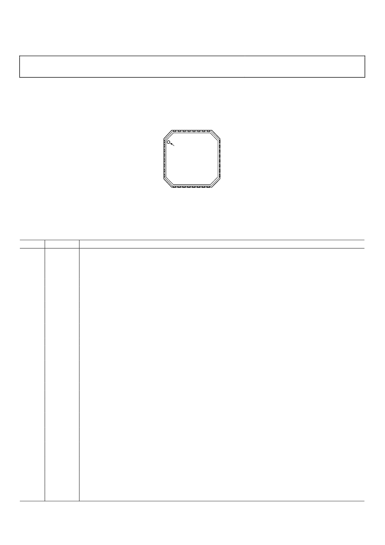
Figure 3. Pin Configuration
Table 4. Pin Function Descriptions
Pin No.
Mnemonic
1
CMR
Description
Common-Mode Reference Voltage for the Differential Amplifier’s Output Voltage Swing. Internally biased to
three-fifths of V
P
3. Requires a 0.1 μF capacitor to ground.
Differential Amplifier Output to Tune the External VCO.
Fast-Lock Switch 3. Closed while SW3 timeout counter is active.
Analog Ground. This is the ground return pin for the differential amplifier and the RF section.
Complementary Input to the RF Prescaler. This point must be decoupled to the ground plane with a small bypass
capacitor, typically 100 pF.
Input to the RF Prescaler. This small signal input is ac-coupled to the external VCO.
Power Supply Pin for the RF Section. Nominally 3 V. A 100 pF decoupling capacitor to the ground plane should be
placed as close as possible to this pin.
Power Supply Pin for the N Divider. Should be the same voltage as AV
DD
1. A 0.1 μF decoupling capacitor to ground
should be placed as close as possible to this pin.
Ground Return Pin for DV
DD
1.
Power Supply Pin for the REF
IN
Buffer and R Divider. Nominally 3 V. A 0.1 μF decoupling capacitor to ground
should be placed as close as possible to this pin.
Reference Input. This is a CMOS input with a nominal threshold of V
DD
/2 and a dc equivalent input resistance of
100 kΩ (see Figure 15). This input can be driven from a TTL or CMOS crystal oscillator or it can be ac-coupled.
Ground Return Pin for DV
DD
2 and DV
DD
3.
Power Supply Pin for the Serial Interface Logic. Nominally 3 V.
Ground Return Pin for the Σ-Δ Modulator.
Power Supply Pin for the Digital Σ-Δ Modulator. Nominally 3 V. A 0.1 μF decoupling capacitor to the ground plane
should be placed as close as possible to this pin.
Multiplexer Output. This multiplexer output allows either the lock detect, the scaled RF, or the scaled reference
frequency to be accessed externally (see Figure 35).
Serial Clock Input. Data is clocked into the 24-bit shift register on the CLK rising edge. This input is a high
impedance CMOS input.
Serial Data Input. The serial data is loaded MSB first with the three LSBs as the control bits. This input is a high
impedance CMOS input.
Load Enable, CMOS Input. When LE goes high, the data stored in the shift register is loaded into the register that is
selected by the three LSBs.
Power Supply Pin for the Phase Frequency Detector (PFD). Nominally 5 V, should be at the same voltage at V
P
2.
A 0.1 μF decoupling capacitor to ground should be placed as close as possible to this pin.
Ground Return Pin for V
P
1.
Ground Return Pin for V
P
2.
2
3
4
5
A
OUT
SW3
A
GND
1
RF
IN
6
7
RF
IN+
AV
DD
1
8
DV
DD
1
9
10
D
GND
1
DV
DD
2
11
REF
IN
12
13
14
15
D
GND
2
DV
DD
3
SD
GND
SDV
DD
16
MUX
OUT
17
CLK
18
DATA
19
LE
20
V
P
1
21
22
D
GND
3
A
GND
2
相關(guān)PDF資料 |
PDF描述 |
|---|---|
| ADF4193BCPZ | Low Phase Noise, Fast Settling PLL Frequency Synthesizer |
| ADF4193BCPZ-RL | Low Phase Noise, Fast Settling PLL Frequency Synthesizer |
| ADF4193BCPZ-RL7 | Low Phase Noise, Fast Settling PLL Frequency Synthesizer |
| ADF4207BRU | Dual RF PLL Frequency Synthesizers |
| ADF4208BRU | Dual RF PLL Frequency Synthesizers |
相關(guān)代理商/技術(shù)參數(shù) |
參數(shù)描述 |
|---|---|
| ADF4193BCPZ | 功能描述:IC PLL FREQ SYNTHESIZER 32LFCSP RoHS:是 類別:集成電路 (IC) >> 時(shí)鐘/計(jì)時(shí) - 時(shí)鐘發(fā)生器,PLL,頻率合成器 系列:- 標(biāo)準(zhǔn)包裝:2,000 系列:- 類型:PLL 頻率合成器 PLL:是 輸入:晶體 輸出:時(shí)鐘 電路數(shù):1 比率 - 輸入:輸出:1:1 差分 - 輸入:輸出:無/無 頻率 - 最大:1GHz 除法器/乘法器:是/無 電源電壓:4.5 V ~ 5.5 V 工作溫度:-20°C ~ 85°C 安裝類型:表面貼裝 封裝/外殼:16-LSSOP(0.175",4.40mm 寬) 供應(yīng)商設(shè)備封裝:16-SSOP 包裝:帶卷 (TR) 其它名稱:NJW1504V-TE1-NDNJW1504V-TE1TR |
| ADF4193BCPZ-RL | 功能描述:IC PLL FREQ SYNTHESIZER 32LFCSP RoHS:是 類別:集成電路 (IC) >> 時(shí)鐘/計(jì)時(shí) - 時(shí)鐘發(fā)生器,PLL,頻率合成器 系列:- 標(biāo)準(zhǔn)包裝:2,000 系列:- 類型:PLL 時(shí)鐘發(fā)生器 PLL:帶旁路 輸入:LVCMOS,LVPECL 輸出:LVCMOS 電路數(shù):1 比率 - 輸入:輸出:2:11 差分 - 輸入:輸出:是/無 頻率 - 最大:240MHz 除法器/乘法器:是/無 電源電壓:3.135 V ~ 3.465 V 工作溫度:0°C ~ 70°C 安裝類型:表面貼裝 封裝/外殼:32-LQFP 供應(yīng)商設(shè)備封裝:32-TQFP(7x7) 包裝:帶卷 (TR) |
| ADF4193BCPZ-RL7 | 功能描述:IC PLL FREQ SYNTHESIZER 32LFCSP RoHS:是 類別:集成電路 (IC) >> 時(shí)鐘/計(jì)時(shí) - 時(shí)鐘發(fā)生器,PLL,頻率合成器 系列:- 標(biāo)準(zhǔn)包裝:2,000 系列:- 類型:PLL 時(shí)鐘發(fā)生器 PLL:帶旁路 輸入:LVCMOS,LVPECL 輸出:LVCMOS 電路數(shù):1 比率 - 輸入:輸出:2:11 差分 - 輸入:輸出:是/無 頻率 - 最大:240MHz 除法器/乘法器:是/無 電源電壓:3.135 V ~ 3.465 V 工作溫度:0°C ~ 70°C 安裝類型:表面貼裝 封裝/外殼:32-LQFP 供應(yīng)商設(shè)備封裝:32-TQFP(7x7) 包裝:帶卷 (TR) |
| ADF4193SP1BCPZ | 制造商:Analog Devices 功能描述: |
| ADF4193SP1BCPZ-RL7 | 制造商:Analog Devices 功能描述: |
發(fā)布緊急采購(gòu),3分鐘左右您將得到回復(fù)。