- 您現在的位置:買賣IC網 > PDF目錄373982 > ADF4193BCPZ-RL7 (ANALOG DEVICES INC) Low Phase Noise, Fast Settling PLL Frequency Synthesizer PDF資料下載
參數資料
| 型號: | ADF4193BCPZ-RL7 |
| 廠商: | ANALOG DEVICES INC |
| 元件分類: | XO, clock |
| 英文描述: | Low Phase Noise, Fast Settling PLL Frequency Synthesizer |
| 中文描述: | PLL FREQUENCY SYNTHESIZER, 3500 MHz, QCC32 |
| 封裝: | 5 X 5 MM, ROHS COMPLIANT, MO-220VHHD-2, LFCSP-32 |
| 文件頁數: | 21/28頁 |
| 文件大小: | 437K |
| 代理商: | ADF4193BCPZ-RL7 |
第1頁第2頁第3頁第4頁第5頁第6頁第7頁第8頁第9頁第10頁第11頁第12頁第13頁第14頁第15頁第16頁第17頁第18頁第19頁第20頁當前第21頁第22頁第23頁第24頁第25頁第26頁第27頁第28頁
ADF4193
MUX REGISTER (R6)
Rev. B | Page 21 of 28
0
DB15
M13
DB14
M12
DB13
M11
DB12
M10
DB11
0
DB10
0
DB9
0
DB8
0
DB7
0
DB6
M4
DB5
M3
DB4
M2
DB3
M1
DB2
C3 (1)
DB1
C2 (1)
DB0
C1 (0)
RESERVED
MUX
OUT
CONTROL
BITS
SIGMA-DELTA
AND
LOCK DETECT MODES
0
1
1
M10
0
1
0
M11
0
0
0
ALL OTHER STATES
M12
0
0
1
M13
INIT STATE, DITHER OFF,
3ns LOCK DETECT THRESHOLD
DITHER ON
10ns LOCK DETECT THRESHOLD
RESERVED
SIGMA-DELTA MODES
0
0
0
0
0
0
0
0
1
1
1
1
1
1
1
1
M4
0
0
0
0
1
1
1
1
0
0
0
0
1
1
1
1
M3
0
0
1
1
0
0
1
1
0
0
1
1
0
0
1
1
M2
0
1
0
1
0
1
0
1
0
1
0
1
0
1
0
1
M1
3-STATE
DIGITAL LOCK DETECT
N DIVIDER OUTPUT
LOGIC HIGH
R COUNTER
RESERVED
SERIAL DATA OUT
LOGIC LOW
R DIVIDER/2 OUTPUT
N DIVIDER/2 OUTPUT
RESERVED
RESERVED
ICP TIMEOUT SIGNAL
SW1/2 TIMEOUT SIGNAL
SW3 TIMEOUT SIGNAL
RESERVED
MUX
OUT
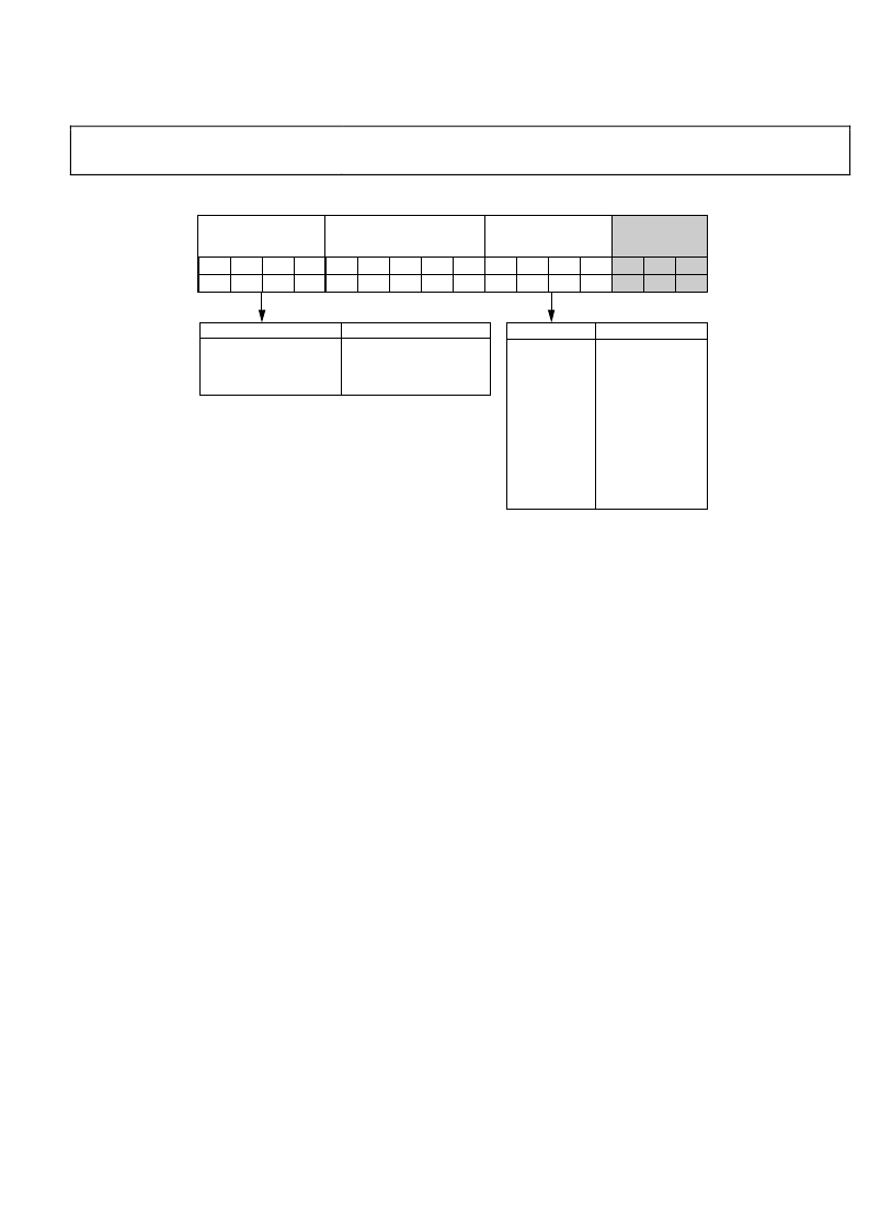
Figure 35. MUX Register (R6)
With C3, C2, and C1 set to 1, 1, 0, respectively, the MUX
register is programmed.
Σ-Δ and Lock Detect Modes
Bit DB15 to Bit DB12 are used to reconfigure certain PLL
operating modes. In the initialization sequence after power is
applied to the chip, the four bits must first be programmed to
all zeros. This initializes the PLL to a known state with dither
off in the Σ-Δ modulator and a 3 ns PFD error threshold in the
lock detect circuit.
To turn on dither in the Σ-Δ modulator, an additional write
should be made to Register R6 to program bits [DB15:DB12] =
[0011]. However, for lowest noise operation, it is best to leave
dither off.
To change the lock detect threshold from 3 ns to 10 ns, a
separate write to R6 should be performed to program bits
[DB15:DB12] = [1001]. This should be done for reliable lock
detect operation when the RF frequency is <2 GHz.
A write to R6 that programs bits [DB15:DB12] = [0000] returns
operation to the default state with both dither off and a 3 ns
lock detect threshold.
Reserved Bits
The reserved bits must all be set to 0 for normal operation.
MUX
OUT
Modes
These bits control the on-chip multiplexer. See Figure 35 for the
truth table. This pin is useful for diagnosis because it allows the
user to look at various internal points of the chip, such as the
R divider and INT divider outputs.
In addition, it is possible to monitor the programmed timeout
counter intervals on MUX
OUT
. For example, if the ICP timeout
counter was programmed to 65 (with a 26 MHz PFD), then
following the next write to R0, a pulse width of 10 μs would be
observed on the MUX
OUT
pin.
Digital lock detect is available via the MUX
OUT
pin.
相關PDF資料 |
PDF描述 |
|---|---|
| ADF4207BRU | Dual RF PLL Frequency Synthesizers |
| ADF4208BRU | Dual RF PLL Frequency Synthesizers |
| ADF4206 | Dual RF PLL Frequency Synthesizers |
| ADF4206BRU | Dual RF PLL Frequency Synthesizers |
| ADF4212 | Dual RF/IF PLL Frequency Synthesizers |
相關代理商/技術參數 |
參數描述 |
|---|---|
| ADF4193SP1BCPZ | 制造商:Analog Devices 功能描述: |
| ADF4193SP1BCPZ-RL7 | 制造商:Analog Devices 功能描述: |
| ADF4193SP2BCPZ-RL7 | 制造商:Analog Devices 功能描述: |
| ADF4193WCCPZ-RL7 | 功能描述:IC PLL FREQ SYNTHESIZER 32LFCSP RoHS:是 類別:集成電路 (IC) >> 時鐘/計時 - 時鐘發生器,PLL,頻率合成器 系列:- 標準包裝:2,000 系列:- 類型:PLL 時鐘發生器 PLL:帶旁路 輸入:LVCMOS,LVPECL 輸出:LVCMOS 電路數:1 比率 - 輸入:輸出:2:11 差分 - 輸入:輸出:是/無 頻率 - 最大:240MHz 除法器/乘法器:是/無 電源電壓:3.135 V ~ 3.465 V 工作溫度:0°C ~ 70°C 安裝類型:表面貼裝 封裝/外殼:32-LQFP 供應商設備封裝:32-TQFP(7x7) 包裝:帶卷 (TR) |
| ADF4196 | 制造商:AD 制造商全稱:Analog Devices 功能描述:Low Phase Noise, Fast Settling, 6 GHz |
發布緊急采購,3分鐘左右您將得到回復。