- 您現在的位置:買賣IC網 > PDF目錄373984 > ADF7020BCP (ANALOG DEVICES INC) High Performance ISM Band FSK/ASK Transceiver IC PDF資料下載
參數資料
| 型號: | ADF7020BCP |
| 廠商: | ANALOG DEVICES INC |
| 元件分類: | 無繩電話/電話 |
| 英文描述: | High Performance ISM Band FSK/ASK Transceiver IC |
| 中文描述: | TELECOM, CELLULAR, RF AND BASEBAND CIRCUIT, QCC48 |
| 封裝: | 7 X 7 MM, LFCSP-48 |
| 文件頁數: | 16/40頁 |
| 文件大小: | 797K |
| 代理商: | ADF7020BCP |
第1頁第2頁第3頁第4頁第5頁第6頁第7頁第8頁第9頁第10頁第11頁第12頁第13頁第14頁第15頁當前第16頁第17頁第18頁第19頁第20頁第21頁第22頁第23頁第24頁第25頁第26頁第27頁第28頁第29頁第30頁第31頁第32頁第33頁第34頁第35頁第36頁第37頁第38頁第39頁第40頁
ADF7020
Preliminary Technical Data
RECEIVER SECTION
RF FRONT END
The ADF7020 is based on a fully integrated, low IF receiver
architecture. The low IF architecture facilitates a very low
external component count and does not suffer from power-line-
induced interference problems.
Rev. PrH | Page 16 of 40
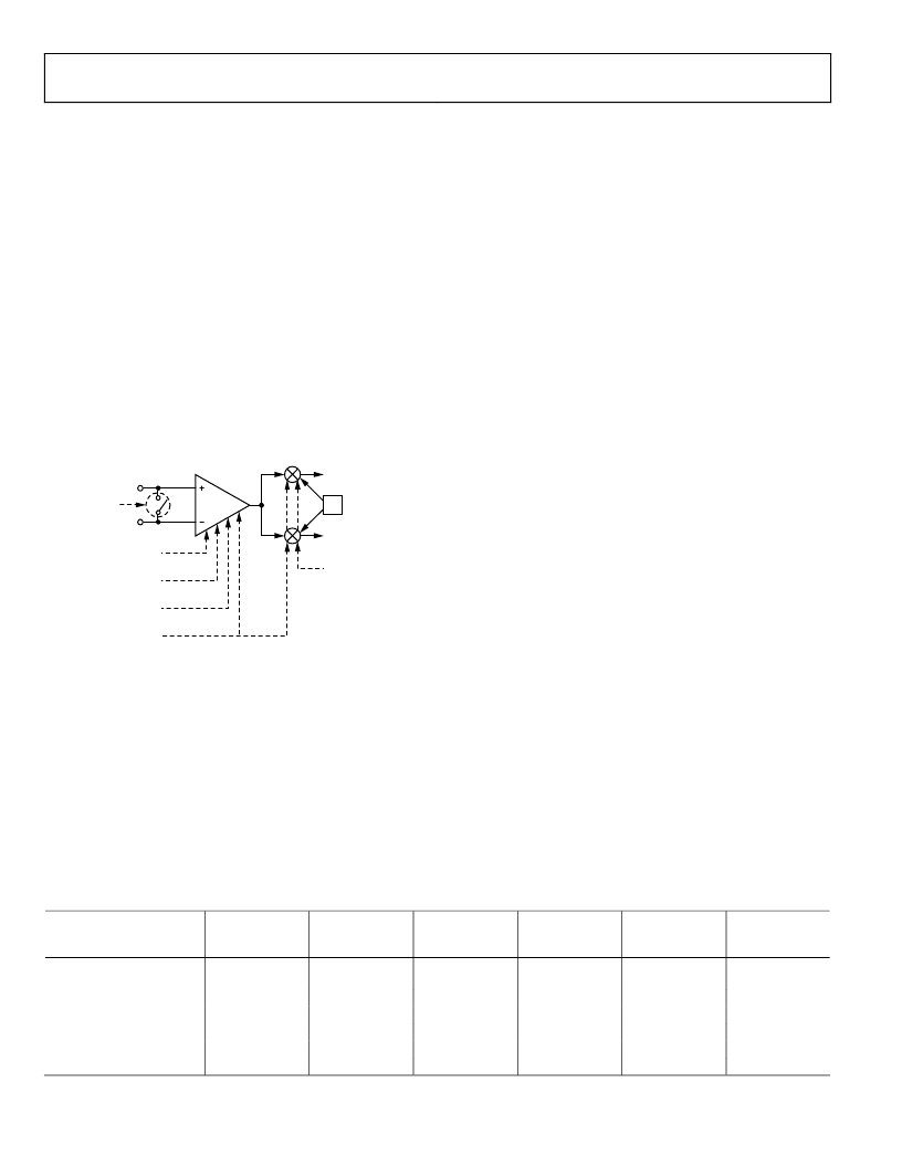
Figure 14 shows the structure of the receiver front end. The
many programming options allow users to trade off sensitivity,
linearity, and current consumption against each other in the
way best suitable for their applications. To achieve a high level
of resilience against spurious reception, the LNA features a
differential input. Switch SW2 shorts the LNA input when
transmit mode is selected (R0_DB27 = 0). This feature
facilitates the design of a combined LNA/PA matching network,
avoiding the need for an external Rx/Tx switch. See the LNA/PA
Matching section for details on the design of the matching
network.
0
SW2
LNA
RFIN
RFINB
Tx/Rx SELECT
[R0_DB27]
LNA MODE
[R6_DB15]
LNA CURRENT
[R6_DB(16:17)]
MIXER LINEARITY
[R6_DB18]
LO
I (TO FILTER)
Q (TO FILTER)
LNA GAIN
[R9_DB(20:21)]
LNA/MIXER ENABLE
[R8_DB6]
Figure 14. ADF7020 RF Front End
The LNA is followed by a quadrature downconversion mixer,
which converts the RF signal to the IF frequency of 200 kHz. It
is important to consider that the output frequency of the
synthesizer must be programmed to a value 200 kHz below the
center frequency of the received channel.
The LNA has two basic operating modes: high gain/low noise
mode and low gain/low power mode. To switch between these
two modes, use the LNA_mode bit, R6_DB15. The mixer is also
configurable between a low current and an enhanced linearity
mode using the mixer_linearity bit, R6_DB18.
Based on the specific sensitivity and linearity requirements of
the application, it is recommended to adjust control bits
LNA_mode (R6_DB15) and mixer_linearity (R6_DB18) as
outlined in Table 5.
The gain of the LNA is configured by the LNA_gain field,
R9_DB(20:21), and can be set by either the user or the AGC
logic.
IF Filter Settings/Calibration
Out-of-band interference is rejected by means of a fourth-order
Butterworth polyphase IF filter centered around a frequency of
200 kHz. The bandwidth of the IF filter can be programmed
between 100 kHz and 200 kHz by means of Control Bits
R1_DB(22:23), and should be chosen as a compromise between
interference rejection, attenuation of the desired signal, and the
AFC pull-in range.
To compensate for manufacturing tolerances, the IF filter
should be calibrated once after power-up. The IF filter
calibration logic requires that the IF filter divider in Bits
R6_DB(20:28) be set dependent on the crystal frequency. Once
initiated by setting Bit R6_DB19, the calibration is performed
automatically without any user intervention. The calibration
time is 200 μs, during which the ADF7020 should not be
accessed. It is important not to initiate the calibration cycle
before the crystal oscillator has fully settled. If the AGC loop is
disabled, the gain of IF filter can be set to three levels using the
filter_gain field, R9_DB(20:21). The filter gain is adjusted
automatically, if the AGC loop is enabled.
The signal in the image channel of the low IF mixer, located at a
frequency of 400 kHz below the desired channel, is rejected due
to the image rejection of the polyphase filter. The image
rejection performance of the IF filter is subject to manufactur-
ing tolerances, and, to some extent, temperature drift. To
improve the image rejection, a calibration procedure can be
performed as outlined in the Image Rejection Calibration
section.
Table 5. LNA/Mixer Modes
Receiver Mode
High Sensitivity Mode
(default)
RxMode2
Low Current Mode
Enhanced Linearity Mode
RxMode5
RxMode6
LNA Mode
(R6_DB15)
0
LNA Gain Value
R9_DB(21:20)
30
Mixer Linearity
(R6_DB18)
0
Sensitivity
(DR = 9.6 kbps,
f
DEV
= 10 kHz)
110.5
Rx Current
Consumption
(mA)
22
Input IP3 (dBm)
35
1
1
1
1
0
10
3
3
10
30
0
0
1
1
1
104
91
101
TBD
TBD
20
19
19
TBD
TBD
15.9
3.2
6.8
8.25
28.8
相關PDF資料 |
PDF描述 |
|---|---|
| ADG1204 | 2 pF Off Capacitance, 1 pC Charge Injection, +-15 V/12 V 4:1 iCMOS Multiplexer |
| ADG1204YCP | 2 pF Off Capacitance, 1 pC Charge Injection, +-15 V/12 V 4:1 iCMOS Multiplexer |
| ADG1204YRU | 2 pF Off Capacitance, 1 pC Charge Injection, +-15 V/12 V 4:1 iCMOS Multiplexer |
| ADG202A | Quad SPST Switches(LC2MOS四單刀單擲開關) |
| ADG201A | Quad SPST Switches(LC2MOS四單刀單擲開關) |
相關代理商/技術參數 |
參數描述 |
|---|---|
| ADF7020BCP-REEL | 制造商:Analog Devices 功能描述:RF TRNSCVR ASK/FSK 2.5V/3.3V 48LFCSP EP - Tape and Reel |
| ADF7020BCP-REEL7 | 制造商:Analog Devices 功能描述:RF TRNSCVR ASK/FSK 2.5V/3.3V 48LFCSP EP - Tape and Reel |
| ADF7020BCP-U1 | 制造商:Analog Devices 功能描述:HIGH PERFORMANCE ISM BAND FSK/ASK TRANSCEIVER IC - Trays |
| ADF7020BCPZ | 功能描述:IC TX FSK/ASK ISM BAND 48LFCSP RoHS:是 類別:RF/IF 和 RFID >> RF 收發器 系列:- 產品培訓模塊:Lead (SnPb) Finish for COTS Obsolescence Mitigation Program 標準包裝:30 系列:- 頻率:4.9GHz ~ 5.9GHz 數據傳輸率 - 最大:54Mbps 調制或協議:* 應用:* 功率 - 輸出:-3dBm 靈敏度:- 電源電壓:2.7 V ~ 3.6 V 電流 - 接收:* 電流 - 傳輸:* 數據接口:PCB,表面貼裝 存儲容量:- 天線連接器:PCB,表面貼裝 工作溫度:-25°C ~ 85°C 封裝/外殼:68-TQFN 裸露焊盤 包裝:管件 |
| ADF7020BCPZ-RL | 功能描述:IC TX FSK/ASK ISM BAND 48LFCSP RoHS:是 類別:RF/IF 和 RFID >> RF 收發器 系列:- 產品培訓模塊:Lead (SnPb) Finish for COTS Obsolescence Mitigation Program 標準包裝:30 系列:- 頻率:4.9GHz ~ 5.9GHz 數據傳輸率 - 最大:54Mbps 調制或協議:* 應用:* 功率 - 輸出:-3dBm 靈敏度:- 電源電壓:2.7 V ~ 3.6 V 電流 - 接收:* 電流 - 傳輸:* 數據接口:PCB,表面貼裝 存儲容量:- 天線連接器:PCB,表面貼裝 工作溫度:-25°C ~ 85°C 封裝/外殼:68-TQFN 裸露焊盤 包裝:管件 |
發布緊急采購,3分鐘左右您將得到回復。