- 您現在的位置:買賣IC網 > PDF目錄373996 > ADM1064 (Analog Devices, Inc.) Super Sequencer with Voltage Readback ADC PDF資料下載
參數資料
| 型號: | ADM1064 |
| 廠商: | Analog Devices, Inc. |
| 英文描述: | Super Sequencer with Voltage Readback ADC |
| 中文描述: | 超級序列與ADC的電壓回讀 |
| 文件頁數: | 25/32頁 |
| 文件大小: | 523K |
| 代理商: | ADM1064 |
第1頁第2頁第3頁第4頁第5頁第6頁第7頁第8頁第9頁第10頁第11頁第12頁第13頁第14頁第15頁第16頁第17頁第18頁第19頁第20頁第21頁第22頁第23頁第24頁當前第25頁第26頁第27頁第28頁第29頁第30頁第31頁第32頁
ADM1064
Rev. 0 | Page 25 of 32
9
0
1
9
9
1
1
9
1
START BY
MASTER
ACK. BY
SLAVE
ACK. BY
MASTER
ACK. BY
MASTER
NO ACK.
FRAME 2
DATA BYTE
FRAME 1
SLAVE ADDRESS
FRAME N
DATA BYTE
FRAME 3
DATA BYTE
SCL
SDA
R/W
STOP
BY
MASTER
SCL
(CONTINUED)
SDA
(CONTINUED)
D7
A0
A1
1
1
1
0
0
D6
D5
D4
D3
D2
D1
D0
D7
D6
D5
D4
D3
D2
D1
D0
D7
D6
D5
D4
D3
D2
D1
D0
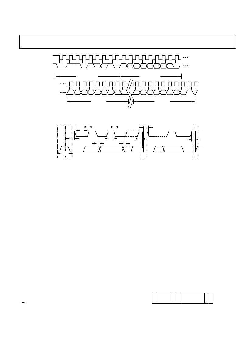
Figure 32. General SMBus Read Timing Diagram
0
SCL
SDA
P
S
S
P
t
SU;STO
t
HD;STA
t
SU;STA
t
SU;DAT
t
HD;DAT
t
HD;STA
t
HIGH
t
BUF
t
LOW
t
R
t
F
Figure 33. Serial Bus Timing Diagram
SMBUS PROTOCOLS FOR RAM AND EEPROM
The ADM1064 contains volatile registers (RAM) and nonvola-
tile registers (EEPROM). User RAM occupies address locations
from 0x00 to 0xDF; EEPROM occupies addresses from 0xF800
to 0xFBFF.
Data can be written to and read from both RAM and EEPROM
as single data bytes. Data can be written only to unprogrammed
EEPROM locations. To write new data to a programmed loca-
tion, it must first be erased. EEPROM erasure cannot be done at
the byte level. The EEPROM is arranged as 32 pages of 32 bytes
each, and an entire page must be erased.
Page erasure is enabled by setting Bit 2 in the UPDCFG register
(Address 0x90) to 1. If this bit is not set, page erasure cannot
occur, even if the command byte (0xFE) is programmed across
the SMBus.
WRITE OPERATIONS
The SMBus specification defines several protocols for different
types of read and write operations. The following abbreviations
are used in the diagrams:
S
P
R
W
A
A
Start
Stop
Read
Write
Acknowledge
No acknowledge
The ADM1064 uses the following SMBus write protocols.
Send Byte
In a send byte operation, the master device sends a single
command byte to a slave device, as follows:
1.
The master device asserts a start condition on SDA.
2.
The master sends the 7-bit slave address followed by the
write bit (low).
3.
The addressed slave device asserts ACK on SDA.
4.
The master sends a command code.
5.
The slave asserts ACK on SDA.
6.
The master asserts a stop condition on SDA and the
transaction ends.
In the ADM1064, the send byte protocol is used for two
purposes:
To write a register address to RAM for a subsequent single
byte read from the same address, or a block read or write
starting at that address, as shown in Figure 34.
0
2
4
1
3
SLAVE
ADDRESS
REGISTER
ADDRESS
(0x00 TO 0xDF)
S
W
A
A
5
6
P
Figure 34. Setting a RAM Address for Subsequent Read
相關PDF資料 |
PDF描述 |
|---|---|
| ADM1064ACP | Super Sequencer with Voltage Readback ADC |
| ADM1064ACP-REEL | Super Sequencer with Voltage Readback ADC |
| ADM1064ACP-REEL7 | Super Sequencer with Voltage Readback ADC |
| ADM1064ASU | Super Sequencer with Voltage Readback ADC |
| ADM1064ASU-REEL | Super Sequencer with Voltage Readback ADC |
相關代理商/技術參數 |
參數描述 |
|---|---|
| ADM1064ACP | 制造商:Analog Devices 功能描述:Volt Supervisor Sequencer 2.7V to 5.4V 40-Pin LFCSP EP |
| ADM1064ACP-REEL | 制造商:Analog Devices 功能描述:Volt Supervisor Sequencer 2.7V to 5.4V 40-Pin LFCSP EP T/R |
| ADM1064ACP-REEL7 | 制造商:Analog Devices 功能描述:Volt Supervisor Sequencer 2.7V to 5.4V 40-Pin LFCSP EP T/R |
| ADM1064ACPZ | 功能描述:IC SEQUENCER/SUPERVISOR 40-LFCSP RoHS:是 類別:集成電路 (IC) >> PMIC - 監控器 系列:Super Sequencer® 標準包裝:1 系列:- 類型:簡單復位/加電復位 監視電壓數目:1 輸出:開路漏極或開路集電極 復位:高有效 復位超時:- 電壓 - 閥值:1.8V 工作溫度:-40°C ~ 125°C 安裝類型:表面貼裝 封裝/外殼:6-TSOP(0.059",1.50mm 寬)5 引線 供應商設備封裝:5-TSOP 包裝:剪切帶 (CT) 其它名稱:NCP301HSN18T1GOSCT |
| ADM1064ASU | 制造商:Analog Devices 功能描述:Volt Supervisor Sequencer 2.7V to 5.4V 48-Pin TQFP |
發布緊急采購,3分鐘左右您將得到回復。