- 您現(xiàn)在的位置:買賣IC網(wǎng) > PDF目錄374004 > ADM5104 (Analog Devices, Inc.) Four-channel FastFast Ethernet 110Base-TX Transceiver(四通道110Base-TX快速以太網(wǎng)收發(fā)器) PDF資料下載
參數(shù)資料
| 型號: | ADM5104 |
| 廠商: | Analog Devices, Inc. |
| 英文描述: | Four-channel FastFast Ethernet 110Base-TX Transceiver(四通道110Base-TX快速以太網(wǎng)收發(fā)器) |
| 中文描述: | 四通道FastFast以太網(wǎng)110Base -得克薩斯州收發(fā)器(四通道110Base -得克薩斯州快速以太網(wǎng)收發(fā)器) |
| 文件頁數(shù): | 6/8頁 |
| 文件大小: | 75K |
| 代理商: | ADM5104 |
a single resistor. A 2.0 V p-p output signal is obtained with an
I
OUT
of 20 mA, corresponding to an Rtxampset = 2280
. Gener-
ally, IOUT = 22.3/Rtxampset.
T he line driver does not share any power supplies or biases with
other blocks or channels in the ADM5104. T his, and techniques
used to stabilize the effective beta of transistors during switching,
keep output common-mode current to <3%.
TECHNICAL
ADM5104
–6–
REV. 0
PRODUCT DE SCRIPT ION
T he ADM5104 provides a single chip solution for interfacing
four 110Base-T X ports to four Category #5 Unshielded T wisted
Pair (UT P) cables. Four channel MII with timing to PMD
transceiver and ASICs will complete four PHY channels for
repeaters/hubs. T he IC provides four independent PMD trans-
ceivers with separate transmit line drivers and receiver buffers
with line equalization and baseline restoration. Each channel has
signal multiplexers that allow the user to independently perform
loopback, signal detect and equalization compensation.
T he line equalization and baseline restoration block compen-
sates for up to 140 M Category #5 UT P and transformer, re-
spectively. T his block has a signal detect output SDOUT n that,
when low, indicates a loss of input signal at Rn
±
.
T he line driver has a differential ECL input stage that provides a
controlled current output to match driving Category #5 UT P
cable. A single resistor for each channel, from the line driver
output current control pin to ground, controls the output cur-
rent. T he user has the option to disable the line driver output. A
signal multiplexer allows the user to loopback the line driver to
the receiver on each respective channel for test purposes.
T HE ORY OF OPE RAT ION
Line Drivers
T he line drivers accept differential input data between 100 mV
and 1.0 V peak (ac coupled or ECL common mode), and
transmits the 125 MHz MLT 3 data signal through a transformer
and up to 100 M of Category #5 Unshielded T wisted Pair cable
(UT P #5) per EIA586A, 802.3 110Base-T X requirements. T he
user sets the output current, I
OUT
, between 4 mA and 40 mA
(cable removed and 100
resistor across the transformer) with
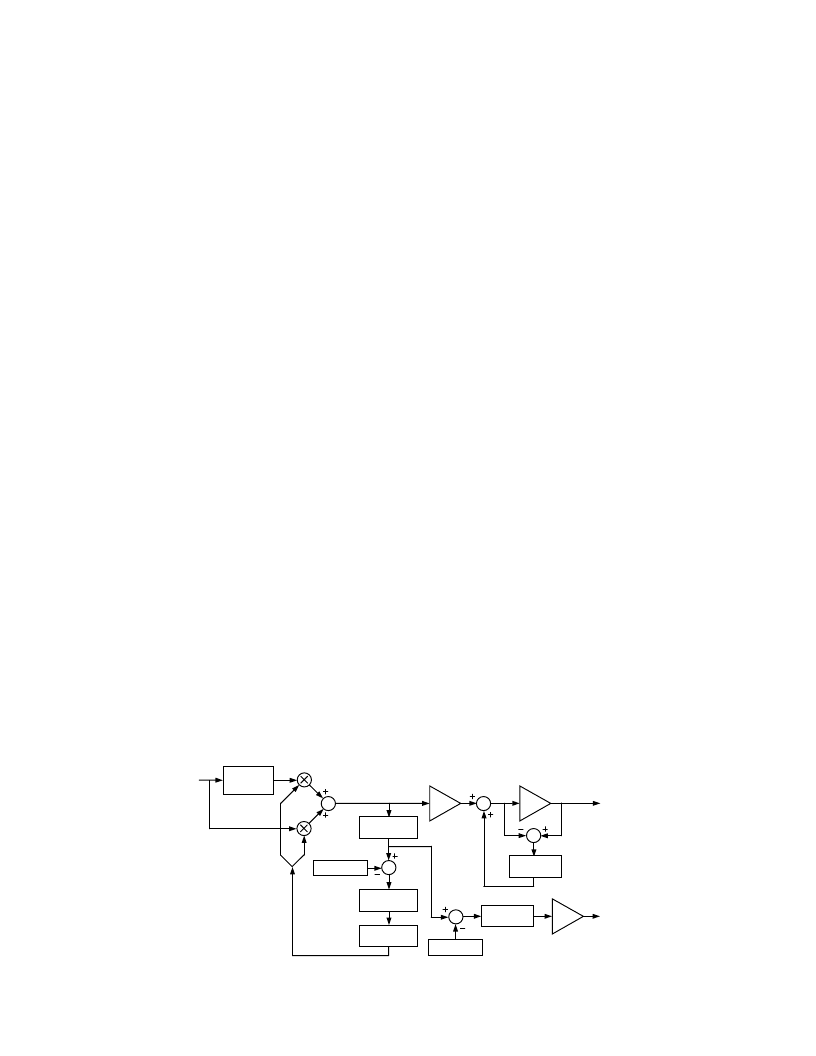
Receiver (E qualizer, Baseline Restoration and Loss of Signal
Detect Circuits)
Each of the four receivers processes an MLT 3 data stream from
a transformer and up to 140 M of Category # 5 Unshielded
T wisted Pair cable (UT P#5). T he receiver (Figure 1) consists
of an adaptive equalizer, a baseline restore loop, and a loss of
signal (LOS) detector. T he adaptive equalizer compensates for
intersymbol interference and distortion caused by the cable. T he
baseline restore loop corrects for baseline wander due to the
coding and transformer. T he LOS detector indicates a cable
break.
T he incoming data chooses either the high pass path, shown as
E(s), the straight path, or some combination of both. T he
strength of each path is determined by the control variable, x.
T he loop works by comparing the amplitude of the equalizer
output to the expected value. If the amplitude is too small, the
signal is under-equalized and the control variable x is decreased
to choose more of the high pass path. T he signal is equalized
when the output amplitude equals the reference value. T he time
constant of the loop is slow enough so that the equalization
remains constant if the signal amplitude decreases due to the
absence of transitions.
T he baseline restore loop compensates for the baseline wander
caused by the transformer (ac coupling) used to terminate the
cable. T his loop adjusts the slice levels of the data signal for
lengthy transitionless data runs to ensure that no bit errors are
made upon new transitions. T his loop also compensates for a dc
offset that could be created by the transformer processing unbal-
anced data signal patterns (baseline wander). T he circuit works
by subtracting the comparator input signal from the output
signal. T he error signal output of the subtracter is added in, to
offset the incoming signal to keep the average value equal to the
average output. If the equalizer output goes to zero, this loop
will servo the comparator input to the last logic level.
T he LOS detector monitors the output amplitude of the equal-
izer and trips when it falls below a predetermined threshold.
T he low-pass filter is slow enough so that the detector will not
trip for less than 800 missing edges.
PE CL Output Compatibility with Fast E thernet PHY Inter-
face IC Inputs
T he PECL outputs (RDn
±
) are more than adequate for driving
interface IC PECL inputs. T his is demonstrated on the com-
parison of the PECL output specifications and an interface IC
PECL input dc characteristics, given below.
T he PECL output levels, specified in single-ended terms over
0
°
C to 70
°
C (V
OH
and V
OL
), should not be taken at face value.
Since the output signals that V
OH
and V
OL
refer to are processed
∑
E(s)
HIFILTER
∑
REFERENCE
LOW-PASS
FILTER
AMPLITUDE
DETECTOR
1-X
X
INTEGRATOR
/ZERO
∑
ADAPTIVE
EQUALIZER
COMP
A
∑
COMP
LOW-PASS
FILTER
LOS
DETECTOR
∑
THRESHOLD
ZERO
RESTORE
LOW-PASS
FILTER
TO CLOCK
RECOVERY
PLL
SDOUT
(LOS)
RX/RXN
DATA INPUT
Figure 1. Receiver Diagram
相關(guān)PDF資料 |
PDF描述 |
|---|---|
| ADM5170AN | 5V High-Speed RS-232 Transceivers with 0.1uF Capacitors |
| ADM5170AP | 5V High-Speed RS-232 Transceivers with 0.1uF Capacitors |
| ADM5170JN | 5V High-Speed RS-232 Transceivers with 0.1uF Capacitors |
| ADM5170JP | 5V High-Speed RS-232 Transceivers with 0.1uF Capacitors |
| ADM5170 | Octal, RS-232/RS-423 Line Driver(八通道,RS-232/RS-423線驅(qū)動器) |
相關(guān)代理商/技術(shù)參數(shù) |
參數(shù)描述 |
|---|---|
| ADM5120 | 制造商:未知廠家 制造商全稱:未知廠家 功能描述:HOME GATEWAY CONTROLLER |
| ADM5120ABT2NP | 制造商:Infineon Technologies AG 功能描述:ROUTER / AP |
| ADM5120PABT2NP | 制造商:Infineon Technologies AG 功能描述:ROUTER / AP |
| ADM5120PX-AB-R-2 | 功能描述:網(wǎng)絡(luò)控制器與處理器 IC ROUTER / ADM RoHS:否 制造商:Micrel 產(chǎn)品:Controller Area Network (CAN) 收發(fā)器數(shù)量: 數(shù)據(jù)速率: 電源電流(最大值):595 mA 最大工作溫度:+ 85 C 安裝風格:SMD/SMT 封裝 / 箱體:PBGA-400 封裝:Tray |
| ADM5120PXABT2 | 制造商:Lantiq 功能描述: |
發(fā)布緊急采購,3分鐘左右您將得到回復(fù)。