- 您現(xiàn)在的位置:買賣IC網(wǎng) > PDF目錄374019 > ADP3025JRU-REEL (ANALOG DEVICES INC) High Efficiency Dual Output Power Supply Controller PDF資料下載
參數(shù)資料
| 型號(hào): | ADP3025JRU-REEL |
| 廠商: | ANALOG DEVICES INC |
| 元件分類: | 穩(wěn)壓器 |
| 英文描述: | High Efficiency Dual Output Power Supply Controller |
| 中文描述: | DUAL SWITCHING CONTROLLER, 350 kHz SWITCHING FREQ-MAX, PDSO38 |
| 封裝: | MO-153BD-1, TSSOP-36 |
| 文件頁(yè)數(shù): | 16/24頁(yè) |
| 文件大小: | 609K |
| 代理商: | ADP3025JRU-REEL |
第1頁(yè)第2頁(yè)第3頁(yè)第4頁(yè)第5頁(yè)第6頁(yè)第7頁(yè)第8頁(yè)第9頁(yè)第10頁(yè)第11頁(yè)第12頁(yè)第13頁(yè)第14頁(yè)第15頁(yè)當(dāng)前第16頁(yè)第17頁(yè)第18頁(yè)第19頁(yè)第20頁(yè)第21頁(yè)第22頁(yè)第23頁(yè)第24頁(yè)

ADP3025
C
IN
AND C
OUT
SELECTION
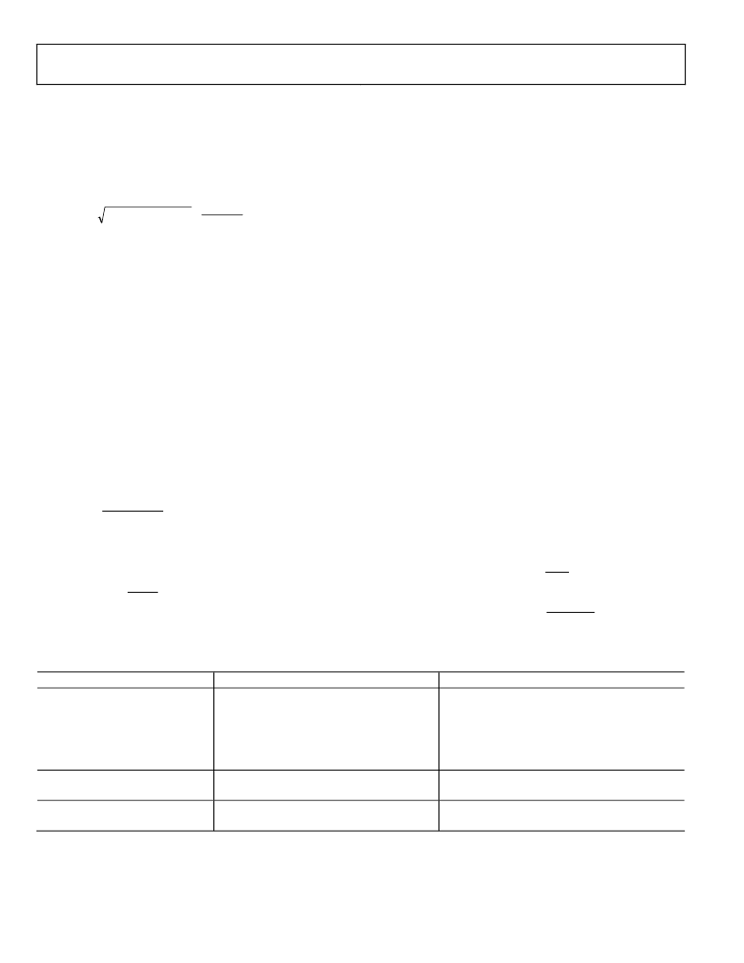
In continuous conduction mode, the source current of the
upper MOSFET is approximately a square wave of duty cycle
V
OUT
/
V
IN
. To prevent large voltage transients, a low ESR input
capacitor sized for the maximum rms current must be used. The
maximum rms capacitor current is
Rev. A | Page 16 of 24
(
)
IN
MAX
OUT
I
OUT
IN
OU
RMS
I
V
V
V
V
T
)
(
×
×
=
(8)
This formula has a maximum at
V
IN
= 2
V
OUT
, where
I
RMS
=
I
OUT
(
MAX
)
/2. Note that the capacitor manufacturer’s ripple current
ratings are often based on only 2,000 hours of life. Therefore,
the user should further derate the capacitor, or choose one rated
at a higher temperature than required. Several capacitors may
be paralleled to meet size or height requirements in the design.
If electrolytic or tantalum capacitors are used, an additional
0.1 μF to 1 μF ceramic bypass capacitor should be placed in
parallel with C
IN
.
The selection of
C
OUT
is driven by the required effective series
resistance (ESR) and the desired output ripple. A good practice
is to limit the ripple voltage to 1% of the nominal output vol-
tage. It is assumed that the total ripple is caused by two factors:
25% comes from the
C
OUT
bulk capacitance value, and 75%
comes from the capacitor ESR. The value of
C
OUT
can be
determined by
RIPPLE
V
RIPPLE
I
×
OUT
f
C
×
=
2
(9)
where
I
RIPPLE
= 0.3 I
OUT
and
V
RIPPLE
= 0.01 V
OUT.
The maximum
acceptable
ESR
of C
OUT
can then be found using
RIPPLE
I
RIPPLE
V
ESR
×
≤
75
.
(10)
Manufacturers such as Vishay, AVX, Elna, WIMA, and Sanyo
provide good high performance capacitors. Sanyo’s OSCON
semiconductor dielectric capacitors have lower ESR for a given
size, at a somewhat higher price. Choosing sufficient capacitors
to meet the ESR requirement for C
OUT
normally exceeds the
amount of capacitance needed to meet the ripple current
requirement.
In surface-mount applications, multiple capacitors may have to
be paralleled to meet the capacitance, ESR, or rms current han-
dling requirements. Aluminum electrolytic and dry tantalum
capacitors are available in surface-mount configurations. In the
case of tantalum, it is critical that capacitors be surge tested for
use in switching power supplies. Recommendations for output
capacitors are shown in Table 8.
POWER MOSFET SELECTION
N-channel power MOSFETs must be selected for use with the
ADP3025 for the main and synchronous switches. The main
selection parameters for the power MOSFETs are the threshold
voltage (V
GS(TH)
) and on resistance (R
DS(ON)
). An internal LDO
generates a 5 V supply that is boosted above the input voltage by
using a bootstrap circuit. This floating 5 V supply is used for the
upper MOSFET gate drive. Logic-level threshold MOSFETs
must be used for both the main and synchronous switches.
Maximum output current (I
MAX
) determines the R
DS(ON)
require-
ment for the two power MOSFETs. When the ADP3025 is
operating in continuous mode, the simplifying assumption can
be made that one of the two MOSFETs is always conducting the
load current. The duty cycles for the MOSFETs are given by
IN
OUT
V
V
Cycle
Duty
MOSFET
Upper
=
(11)
IN
OUT
IN
V
V
V
Cycle
Duty
MOSFET
Lower
=
(12)
Table 8. Recommended Capacitor Manufacturers
Maximum Output Current
Input Capacitors
2 A
TOKIN Multilayer
Ceramic Caps, 22 μF/25 V
P/N: C55Y5U1E226Z
TAIYO YUDEN INC.
Ceramic Caps, Y5V Series 10 μF/25 V
P/N: TMK432BJ106KM
SANYO POSCAP TPC
Series, 68 μF/10 V
SANYO POSCAP TPC
Series, 68 μF/10 V
4 A
TOKIN Multilayer
Ceramic Caps, 2 × 22 μF/25 V
P/N: C55Y5U1E226Z
TAIYO YUDEN INC.
Ceramic Caps, Y5V Series 2 × 10 μF/25 V
P/N: TMK432BJ106KM
SANYO POSCAP TPC
Series, 2 × 68 μF/10 V
SANYO POSCAP TPC
Series, 2 × 68 μF/10 V
Output Capacitors
3.3 V Output
Output Capacitors
5 V Output
相關(guān)PDF資料 |
PDF描述 |
|---|---|
| ADP3025 | High Efficiency Dual Output Power Supply Controller |
| ADP3050AR-33 | Circular Connector Cable Assembly; Connector Type A:Circular Plug; Connector Type B:Stripped End Leads; Cable Length:10ft RoHS Compliant: Yes |
| ADP3050AR-5 | Circular Connector Cable Assembly; Connector Type A:Circular Receptacle; Connector Type B:Stripped End Leads; Cable Length:10ft RoHS Compliant: Yes |
| ADP3050 | 200 kHz, 1 A High-Voltage Step-Down Switching Regulator |
| ADP3050AR | 200 kHz, 1 A High-Voltage Step-Down Switching Regulator |
相關(guān)代理商/技術(shù)參數(shù) |
參數(shù)描述 |
|---|---|
| ADP3025JRUZ-REEL | 制造商:Rochester Electronics LLC 功能描述: 制造商:Analog Devices 功能描述: |
| ADP3026 | 制造商:AD 制造商全稱:Analog Devices 功能描述:High-Efficiency Notebook Computer Power Supply Controller |
| ADP3026ARU | 制造商:AD 制造商全稱:Analog Devices 功能描述:High-Efficiency Notebook Computer Power Supply Controller |
| ADP3026JRUZ-REEL | 制造商:Rochester Electronics LLC 功能描述:DUAL OUTPUT SYNCHRNOUS BUCK CONTROLLER - Tape and Reel 制造商:Analog Devices 功能描述: |
| ADP3031 | 制造商:AD 制造商全稱:Analog Devices 功能描述:2 MHz PWM Boost Switching Regulator |
發(fā)布緊急采購(gòu),3分鐘左右您將得到回復(fù)。