- 您現在的位置:買賣IC網 > PDF目錄374019 > ADP3025JRU-REEL (ANALOG DEVICES INC) High Efficiency Dual Output Power Supply Controller PDF資料下載
參數資料
| 型號: | ADP3025JRU-REEL |
| 廠商: | ANALOG DEVICES INC |
| 元件分類: | 穩壓器 |
| 英文描述: | High Efficiency Dual Output Power Supply Controller |
| 中文描述: | DUAL SWITCHING CONTROLLER, 350 kHz SWITCHING FREQ-MAX, PDSO38 |
| 封裝: | MO-153BD-1, TSSOP-36 |
| 文件頁數: | 18/24頁 |
| 文件大小: | 609K |
| 代理商: | ADP3025JRU-REEL |
ADP3025
2.
Rev. A | Page 18 of 24
Switching losses due to the limited time of switching
transitions. This occurs due to gate drive losses of the
upper and lower MOSFETs and the switching node
capacitive losses, and through hysteresis and eddy-current
losses in power choke. Input and output capacitor ripple
current losses should also be considered switching losses.
These losses are input voltage dependent and can be
estimated as follows:
(19)
f
C
I
V
P
SN
MAX
IN
SWLOSS
×
×
×
=
85
.
where
C
SN
is the overall capacitance of the switching node
related to loss.
3.
Supply current of the switching controller (independent of
the input current redirected to supply the MOSFETs’ gates).
This is a very small portion of the overall loss, but it does
increase with input voltage.
TRANSIENT RESPONSE CONSIDERATIONS
Both stability and regulator loop response can be checked by
looking at the load transient response. Switching regulators take
several cycles to respond to a step in output load current. When
a load step occurs, output voltage shifts by an amount equal to
the current step multiplied by the total ESR of the summed
output capacitor array. Output overshoot or ringing during the
recovery time (in both directions of the current step change)
indicates a stability problem. The external feedback compensa-
tion components shown in Figure 17 should provide adequate
compensation for most applications.
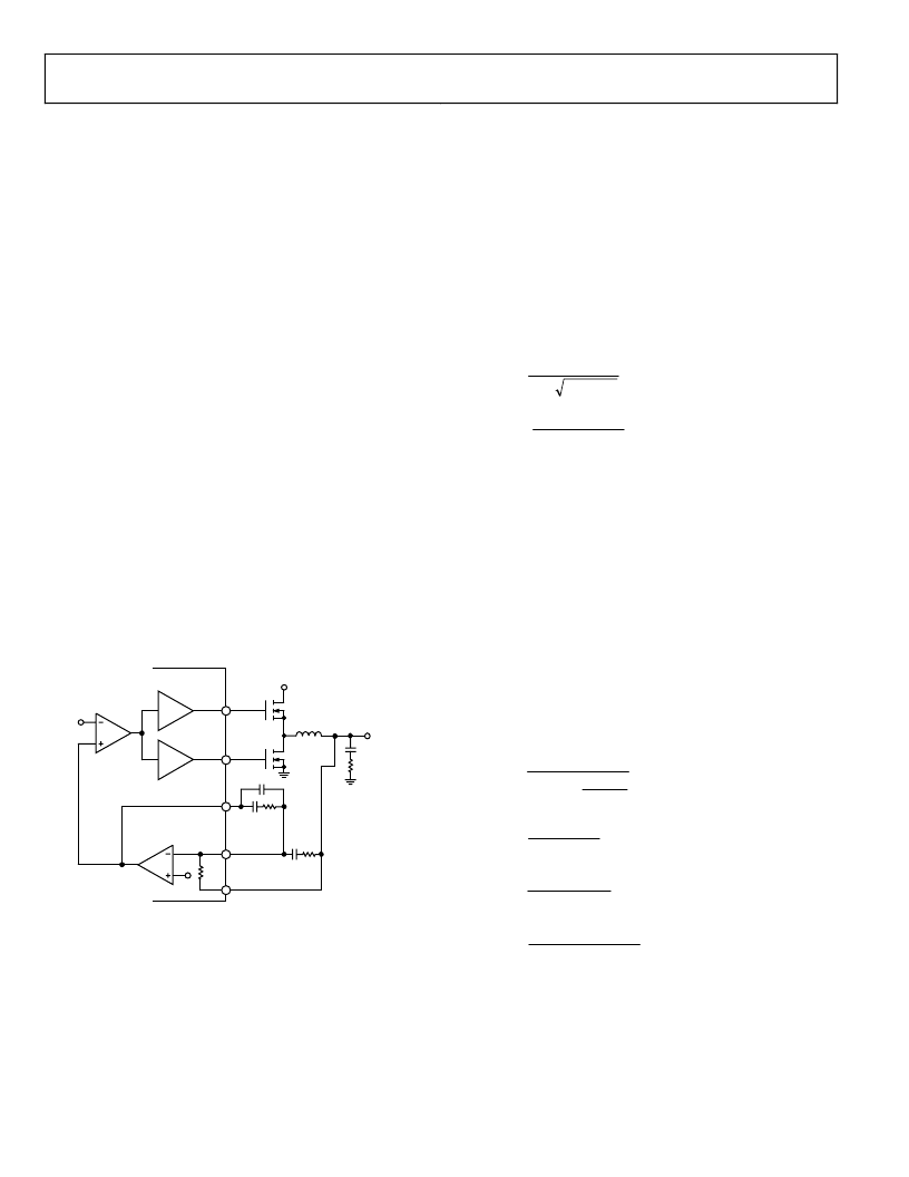
V
OUT
C
OUT
L1
PWM
COMPARATOR
ADP3025
VIN
DRVH
DRVL
PARASITIC
ESR
EAO
EAN
REF
R1
FB
R3
C1
C2
C3
R2
V
RAMP
0
Figure 18. Buck Regulator Voltage Control Loop
FEEDBACK LOOP COMPENSATION
The ADP3025 uses voltage mode control to stabilize the
switching controller outputs. Figure 18 shows the voltage mode
control loop for one of the buck switching regulators. The inter-
nal reference voltage, V
REF
, is applied to the positive input of the
internal error amplifier. The other input of the error amplifier is
EAN, and is internally connected to the feedback sensing pin,
FB, via an internal resistor. The error amplifier creates the
closed-loop voltage level for the pulse-width modulator that
drives the external power MOSFETs. The output LC filter
smoothes the pulse-width modulated input voltage to a dc
output voltage.
The pulse-width modulator transfer function is V
OUT
/V
EAOUT
,
where V
EAOUT
is the output voltage of the error amplifier. That
function is dominated by the impedance of the output filter
with its double-pole resonance frequency (f
LC
), a single zero at
the output capacitor (f
ESR
), and the dc gain of the modulator; it
is equal to the input voltage divided by the peak ramp height
(V
RAMP
), which is equal to 1.2 V when VIN = 12 V.
OUT
F
LC
f
C
L
×
×
π
=
2
1
(20)
OUT
ESR
f
C
ESR
×
×
π
=
2
1
(21)
The compensation network consists of the internal error
amplifier and two external impedance networks, Z
IN
and Z
FB
.
Once the application and the output filter capacitance and ESR
are chosen, the specific component values of the external
impedance networks, Z
IN
and Z
FB
, can be determined. There are
two design criteria for achieving stable switching regulator
behavior within the line and load range. One is the maximum
bandwidth of the loop, which affects fast transient response, if
needed; the other is the minimum accepted by the design phase
margin.
The phase margin is the difference between the closed-loop
phase and 180°. Recommended phase margin is 45° to 60° for
most applications.
The equations to calculate the compensation poles and zeros are
2
C
1
C
2
C
1
C
2
R
f
1
P
+
×
×
×
π
=
2
1
(22)
3
C
3
R
f
2
P
×
×
π
=
2
1
(23)
1
C
2
R
f
1
Z
×
×
π
=
2
1
(24)
(
)
3
C
3
R
1
R
f
2
Z
×
×
×
π
=
2
1
(25)
The value of the internal resistor
R1
is 74 k for the 3.3 V
switching regulator and 130 k for the 5 V switching regulator.
相關PDF資料 |
PDF描述 |
|---|---|
| ADP3025 | High Efficiency Dual Output Power Supply Controller |
| ADP3050AR-33 | Circular Connector Cable Assembly; Connector Type A:Circular Plug; Connector Type B:Stripped End Leads; Cable Length:10ft RoHS Compliant: Yes |
| ADP3050AR-5 | Circular Connector Cable Assembly; Connector Type A:Circular Receptacle; Connector Type B:Stripped End Leads; Cable Length:10ft RoHS Compliant: Yes |
| ADP3050 | 200 kHz, 1 A High-Voltage Step-Down Switching Regulator |
| ADP3050AR | 200 kHz, 1 A High-Voltage Step-Down Switching Regulator |
相關代理商/技術參數 |
參數描述 |
|---|---|
| ADP3025JRUZ-REEL | 制造商:Rochester Electronics LLC 功能描述: 制造商:Analog Devices 功能描述: |
| ADP3026 | 制造商:AD 制造商全稱:Analog Devices 功能描述:High-Efficiency Notebook Computer Power Supply Controller |
| ADP3026ARU | 制造商:AD 制造商全稱:Analog Devices 功能描述:High-Efficiency Notebook Computer Power Supply Controller |
| ADP3026JRUZ-REEL | 制造商:Rochester Electronics LLC 功能描述:DUAL OUTPUT SYNCHRNOUS BUCK CONTROLLER - Tape and Reel 制造商:Analog Devices 功能描述: |
| ADP3031 | 制造商:AD 制造商全稱:Analog Devices 功能描述:2 MHz PWM Boost Switching Regulator |
發布緊急采購,3分鐘左右您將得到回復。