- 您現(xiàn)在的位置:買賣IC網(wǎng) > PDF目錄374019 > ADP3025JRU-REEL (ANALOG DEVICES INC) High Efficiency Dual Output Power Supply Controller PDF資料下載
參數(shù)資料
| 型號: | ADP3025JRU-REEL |
| 廠商: | ANALOG DEVICES INC |
| 元件分類: | 穩(wěn)壓器 |
| 英文描述: | High Efficiency Dual Output Power Supply Controller |
| 中文描述: | DUAL SWITCHING CONTROLLER, 350 kHz SWITCHING FREQ-MAX, PDSO38 |
| 封裝: | MO-153BD-1, TSSOP-36 |
| 文件頁數(shù): | 6/24頁 |
| 文件大小: | 609K |
| 代理商: | ADP3025JRU-REEL |
ADP3025
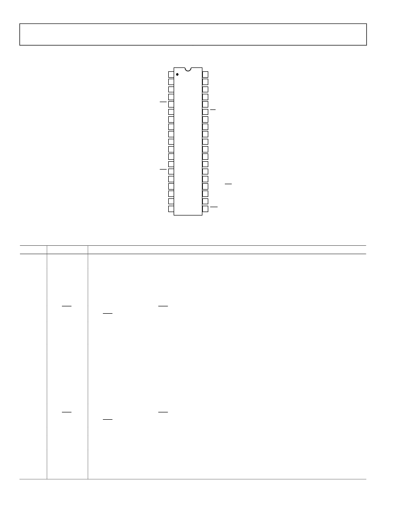
PIN CONFIGURATION AND FUNCTION DESCRIPTIONS
Rev. A | Page 6 of 24
13
18
14
12
11
10
9
8
1
2
3
4
7
6
5
19
17
16
15
20
29
28
27
32
31
30
38
37
36
35
34
33
23
22
21
26
25
24
TOP VIEW
(Not to Scale)
ADP3025
BST5
DRVH5
SW5
DRVL5
PGND1
SD
PGND2
INTVCC1
VIN
DRVL3
SW3
DRVH3
BST3
DRV2
FB2
COMP2/SD2
CPOR
PWRGD
CS5
FB5
EAN5
EAO5
PFI
SS5
CLSET5
REF
AGND
CLSET3
INTVCC2
SYNC
SS3
PFO
EAO3
EAN3
FB3
CS3
ADJ/FX3
ADJ/FX5
0
Figure 2. 38-Lead TSSOP Pin Configuration
Table 3. Pin Function Descriptions
Pin No.
Mnemonic
1
CS5
Function
Current Sense Input for the Top N-Channel MOSFET of the 5 V Buck Converter. Connect to the drain of the top
N-channel MOSFET.
Feedback Input for the 5 V Buck Converter. Connect to the output sense point in fixed output mode. Connect to
an external resistor divider in adjustable output mode.
Inverting Input of the Error Amplifier of the 5 V Buck Converter. Use for external loop compensation only in
fixed output mode. In adjustable output mode, connect to the external resistor divider.
Error Amplifier Output for the 5 V Buck Converter.
TTL Logic Input. When ADJ/FX5 = 0 V, fixed output mode, connect FB5 to the output sense point. When
ADJ/FX5 = 5 V, adjustable output mode, connect FB5 to the external resistor divider.
Soft Start for the 5 V Buck Converter. Also used as an ON/OFF pin.
Current Limit Setting. A resistor can be connected from AGND to CLSET5. A minimum current limit is obtained
by leaving it open. A maximum current limit is obtained by connecting it to AGND.
800 mV Reference. Bypass it with a capacitor (22 nF typical) to AGND. REF cannot be loaded externally.
Analog Signal Ground.
Current Limit Setting. A resistor can be connected from AGND to CLSET3. A minimum current limit is obtained
by leaving it open. A maximum current limit is obtained by connecting it to AGND.
Linear Regulator Bypass for the Internal 5 V LDO. Bypass this pin with a 4.7 μF capacitor to AGND. Pins 11 and 31
must be connected for proper operation.
Oscillator Synchronization and Frequency Select. f
OSC
= 200 kHz when SYNC = 0 V; select f
OSC
= 300 kHz, when
SYNC = 5 V. The oscillator can be synchronized with an external source through the SYNC pin.
Soft Start for the 3.3 V Buck Converter. Also used as an ON/OFF pin.
TTL Logic Input. When ADJ/FX3 = 0 V, fixed output mode, connect FB3 to the output sense point. When
ADJ/FX3 = 5 V, adjustable output mode, connect FB3 to the external resistor divider.
Error Amplifier Output for the 3.3 V Buck Converter.
Error Amplifier Inverting Input of the 3.3 V Buck Converter. Use for external loop compensation only in fixed
output mode. In adjustable output mode, connect to an external resistor divider.
Feedback Input for the 3.3 V Buck Converter. Connect to output sense point in fixed output mode. Connect to
an external resistor divider in adjustable output mode.
Current Sense Input for the Top N-Channel MOSFET of the 3.3 V Buck Converter. CS3 should be connected to
the drain of the N-channel MOSFET.
2
FB5
3
EAN5
4
5
EAO5
ADJ/FX5
6
7
SS5
CLSET5
8
9
10
REF
AGND
CLSET3
11, 31
INTVCC2, 1
12
SYNC
13
14
SS3
ADJ/FX3
15
16
EAO3
EAN3
17
FB3
18
CS3
相關(guān)PDF資料 |
PDF描述 |
|---|---|
| ADP3025 | High Efficiency Dual Output Power Supply Controller |
| ADP3050AR-33 | Circular Connector Cable Assembly; Connector Type A:Circular Plug; Connector Type B:Stripped End Leads; Cable Length:10ft RoHS Compliant: Yes |
| ADP3050AR-5 | Circular Connector Cable Assembly; Connector Type A:Circular Receptacle; Connector Type B:Stripped End Leads; Cable Length:10ft RoHS Compliant: Yes |
| ADP3050 | 200 kHz, 1 A High-Voltage Step-Down Switching Regulator |
| ADP3050AR | 200 kHz, 1 A High-Voltage Step-Down Switching Regulator |
相關(guān)代理商/技術(shù)參數(shù) |
參數(shù)描述 |
|---|---|
| ADP3025JRUZ-REEL | 制造商:Rochester Electronics LLC 功能描述: 制造商:Analog Devices 功能描述: |
| ADP3026 | 制造商:AD 制造商全稱:Analog Devices 功能描述:High-Efficiency Notebook Computer Power Supply Controller |
| ADP3026ARU | 制造商:AD 制造商全稱:Analog Devices 功能描述:High-Efficiency Notebook Computer Power Supply Controller |
| ADP3026JRUZ-REEL | 制造商:Rochester Electronics LLC 功能描述:DUAL OUTPUT SYNCHRNOUS BUCK CONTROLLER - Tape and Reel 制造商:Analog Devices 功能描述: |
| ADP3031 | 制造商:AD 制造商全稱:Analog Devices 功能描述:2 MHz PWM Boost Switching Regulator |
發(fā)布緊急采購,3分鐘左右您將得到回復(fù)。