- 您現在的位置:買賣IC網 > PDF目錄374033 > ADSP-21365 (Analog Devices, Inc.) SHARC Processor PDF資料下載
參數資料
| 型號: | ADSP-21365 |
| 廠商: | Analog Devices, Inc. |
| 元件分類: | 數字信號處理 |
| 英文描述: | SHARC Processor |
| 中文描述: | SHARC處理器 |
| 文件頁數: | 17/54頁 |
| 文件大小: | 559K |
| 代理商: | ADSP-21365 |
第1頁第2頁第3頁第4頁第5頁第6頁第7頁第8頁第9頁第10頁第11頁第12頁第13頁第14頁第15頁第16頁當前第17頁第18頁第19頁第20頁第21頁第22頁第23頁第24頁第25頁第26頁第27頁第28頁第29頁第30頁第31頁第32頁第33頁第34頁第35頁第36頁第37頁第38頁第39頁第40頁第41頁第42頁第43頁第44頁第45頁第46頁第47頁第48頁第49頁第50頁第51頁第52頁第53頁第54頁
ADSP-21365/6
Preliminary Technical Data
Rev. PrA
|
Page 17 of 54
|
September 2004
(PLL). This PLL-based clocking minimizes the skew between
the system clock (CLKIN) signal and the processor’s internal
clock (the clock source for the parallel port logic and I/O pads).
Note the definitions of various clock periods that are a function
of CLKIN and the appropriate ratio control (
Table 8
).
Figure 5
shows Core to CLKIN ratios of 6:1, 16:1 and 32:1 with
external oscillator or crystal. Note that more ratios are possible
and can be set through software using the power management
control register (PMCTL). For more information, see the
ADSP-
2136x SHARC Processor Programming Reference
.
Use the exact timing information given. Do not attempt to
derive parameters from the addition or subtraction of others.
While addition or subtraction would yield meaningful results
for an individual device, the values given in this data sheet
reflect statistical variations and worst cases. Consequently, it is
not meaningful to add parameters to derive longer times. See
Figure 38 on page 43
under Test Conditions for voltage refer-
ence levels.
Switching Characteristics
specify how the processor changes its
signals. Circuitry external to the processor must be designed for
compatibility with these signal characteristics. Switching char-
acteristics describe what the processor will do in a given
circumstance. Use switching characteristics to ensure that any
timing requirement of a device connected to the processor (such
as memory) is satisfied.
Timing Requirements
apply to signals that are controlled by cir-
cuitry external to the processor, such as the data input for a read
operation. Timing requirements guarantee that the processor
operates correctly with other devices.
Table 8. ADSP-21365/6 CLKOUT and CCLK Clock
Generation Operation
Timing
Requirements
CLKIN
CCLK
Description
Calculation
Input Clock
Core Clock
1/t
CK
1/t
CCLK
Table 9. Clock Periods
Timing
Requirements
t
CK
t
CCLK
t
PCLK
t
SCLK
t
SPICLK
Description
1
1
where:
SR = serial port-to-core clock ratio (wide range, determined by SPORT
CLKDIV)
SPIR = SPI-to-Core Clock Ratio (wide range, determined by SPIBAUD register)
DAI_Px = Serial Port Clock
SPICLK = SPI Clock
CLKIN Clock Period
(Processor) Core Clock Period
(Peripheral) Clock Period = 2 × t
CCLK
Serial Port Clock Period = (t
PCLK
) × SR
SPI Clock Period = (t
PCLK
) × SPIR
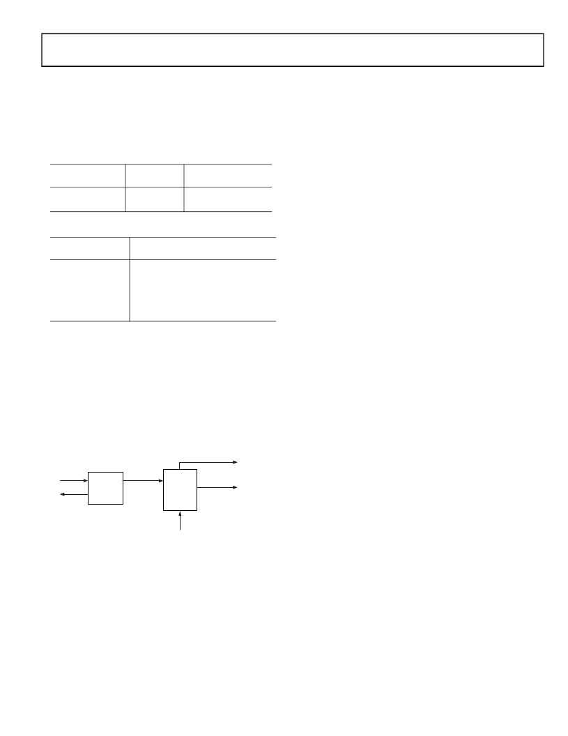
Figure 5. Core Clock and System Clock Relationship to CLKIN
CLKIN
CCLK
(CORECLOCK)
PLLILCLK
XTAL
XTAL
OSC
PLL
6:1, 16:1,
32:1
CLKOUT
CLK-CFG[1:0]
相關PDF資料 |
PDF描述 |
|---|---|
| ADSP-21365SBBC-ENG | SHARC Processor |
| ADSP-21365SBBCZENG | SHARC Processor |
| ADSP-21365SBSQ-ENG | SHARC Processor |
| ADSP-21365SKBCZENG | SHARC Processor |
| ADSP-21365SKSQZENG | SHARC Processor |
相關代理商/技術參數 |
參數描述 |
|---|---|
| ADSP-21365BBC-1AA | 制造商:Analog Devices 功能描述:DSP Floating-Point 32-Bit/40-Bit 333MHz 333MIPS 136-Pin CSP-BGA |
| ADSP-21365BBCZ-1AA | 功能描述:IC DSP 32BIT 333MHZ 136-CSPBGA RoHS:是 類別:集成電路 (IC) >> 嵌入式 - DSP(數字式信號處理器) 系列:SHARC® 標準包裝:2 系列:StarCore 類型:SC140 內核 接口:DSI,以太網,RS-232 時鐘速率:400MHz 非易失內存:外部 芯片上RAM:1.436MB 電壓 - 輸入/輸出:3.30V 電壓 - 核心:1.20V 工作溫度:-40°C ~ 105°C 安裝類型:表面貼裝 封裝/外殼:431-BFBGA,FCBGA 供應商設備封裝:431-FCPBGA(20x20) 包裝:托盤 |
| ADSP-21365BSWZ-1AA | 功能描述:IC DSP 32BIT 333MHZ EPAD 144LQFP RoHS:是 類別:集成電路 (IC) >> 嵌入式 - DSP(數字式信號處理器) 系列:SHARC® 標準包裝:2 系列:StarCore 類型:SC140 內核 接口:DSI,以太網,RS-232 時鐘速率:400MHz 非易失內存:外部 芯片上RAM:1.436MB 電壓 - 輸入/輸出:3.30V 電壓 - 核心:1.20V 工作溫度:-40°C ~ 105°C 安裝類型:表面貼裝 封裝/外殼:431-BFBGA,FCBGA 供應商設備封裝:431-FCPBGA(20x20) 包裝:托盤 |
| ADSP-21365KBC-1AA | 制造商:Analog Devices 功能描述:DSP Floating-Point 32-Bit/40-Bit 333MHz 333MIPS 136-Pin CSP-BGA |
| ADSP-21365KBCZ1AA | 制造商:Analog Devices 功能描述:DSP FLOATING PT 32BIT/40-BIT 333MHZ 333MIPS 136CSPBGA - Trays |
發布緊急采購,3分鐘左右您將得到回復。